- Forums
- Product Forums
- General Purpose MicrocontrollersGeneral Purpose Microcontrollers
- i.MX Forumsi.MX Forums
- QorIQ Processing PlatformsQorIQ Processing Platforms
- Identification and SecurityIdentification and Security
- Power ManagementPower Management
- MCX Microcontrollers
- S32G
- S32K
- S32V
- MPC5xxx
- Other NXP Products
- Wireless Connectivity
- S12 / MagniV Microcontrollers
- Powertrain and Electrification Analog Drivers
- Sensors
- Vybrid Processors
- Digital Signal Controllers
- 8-bit Microcontrollers
- ColdFire/68K Microcontrollers and Processors
- PowerQUICC Processors
- OSBDM and TBDML
- S32M
-
- Solution Forums
- Software Forums
- MCUXpresso Software and ToolsMCUXpresso Software and Tools
- CodeWarriorCodeWarrior
- MQX Software SolutionsMQX Software Solutions
- Model-Based Design Toolbox (MBDT)Model-Based Design Toolbox (MBDT)
- FreeMASTER
- eIQ Machine Learning Software
- Embedded Software and Tools Clinic
- S32 SDK
- S32 Design Studio
- GUI Guider
- Zephyr Project
- Voice Technology
- Application Software Packs
- Secure Provisioning SDK (SPSDK)
- Processor Expert Software
- MCUXpresso Training Hub
-
- Topics
- Mobile Robotics - Drones and RoversMobile Robotics - Drones and Rovers
- NXP Training ContentNXP Training Content
- University ProgramsUniversity Programs
- Rapid IoT
- NXP Designs
- SafeAssure-Community
- OSS Security & Maintenance
- Using Our Community
-
- Cloud Lab Forums
-
- Knowledge Bases
- ARM Microcontrollers
- i.MX Processors
- Identification and Security
- Model-Based Design Toolbox (MBDT)
- QorIQ Processing Platforms
- S32 Automotive Processing Platform
- Wireless Connectivity
- CodeWarrior
- MCUXpresso Suite of Software and Tools
- MQX Software Solutions
-
Hello,
Correct, the pin 9 should be left disconnected/floating. Can you please try to disconnect it?
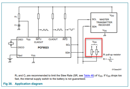
Another thing, the SDA and SCL lines should have connected a resistor on pull-up. Could you please double check that?
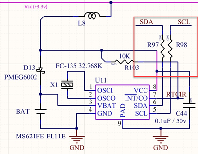
In your schematic, they don’t look to be on pull-up. Also, what size of resistors are you connecting to SDA and SCL?
We need to check if this can be a hardware issue with the device.
Have a great day,
Paulina
Hi Paulina,
Thanks for your reply. Sorry for the delayed response, I was super busy in this week with office work.
I will try to remove GND connection from Pin 9 and get back to you. (but its difficult, because of very tiny package).
Note:
a. SDA are SCL are pulled-up with 3K9 resistance, if not we can't able to get such wave forms (what i have attached in first mail). Am I correct..?
b. I have connected 6, I2C devices with different slave addresses in this same bus, they are all works good [acknowledged and performed as expected].
thanks and regards,
Mani
Hello,
Yes. However, the wave forms showed in your screenshot has some picks that can be noise. Please make sure that the resistors for the SDA and SCL lines are pull-up (connected to VDD as shown in the picture below) as per looking your schematic doesn’t look like they are pull-up.
Have a great day,
Paulina
Hi Paulina,
Thanks for your info. I'm very sure, I'm using 3K9 pull-up to Vcc (_+3v3).
All other I2C devices are working well as intended without any issue.
I'm facing issue only with this chip. In above schematic R97 and R98 are 0 Ohms resistor for terminating purpose, I have added in my schematic.
The SDA and SCL lines are tied with I2C Bus.
FYI: I'm not yet tried with removing GND from pin 9, because it need a re-work. I have ordered couple Chips, I'm very sure the present chip will be damaged while removing from PCB. Once I have received new chips, then I will start to removing the existing chip from my Board and do the test.
I will be keep you posted, if anything turned well.
Thanks and regards,
Mani
Hello Mani,
Sure, please keep me posted with any finding on your side.
Have a great day,
Paulina
Hi Paulina,
Sorry for the delayed reply. I was super busy with office work.
I hope I have identified the fault. The fault was while creating symbol I have swapped the SCL and SDA line..
You can See in the above circuit diagram itself.
I have ordered small Piggy board [top- to-solder]. I will test it once PCB received.
thanks and regards,
Mani
Hi Paulina,
Thanks for your reply and suggestion.
I didn't wait for 2 sec, I will check and come back as soon as I can.
but I'm very sure, I have followed as mentioned in datasheet 8.11.5 and within the limits mentioned in table 49.
I have one more question.
I had a connection in pin 9 (exposed Pad) with GND, does it make any issue.? because we have note on page 5 in the datasheet as "[3]The die paddle (exposed pad) is connected to VSS and should be electrically isolated."
Thanks and regards,
Mani
Hi Paulina,
I have checked with more than 2 sec delayed after powered up. there is no change.. same as "Not acknowledge".
please share your clarification.
Thanks and Regards,
Mani
Hi Paulina,
I forgot to inform you, I can have square wave pulses in pin INT/OUT. In this mean the oscillator work fine right..?.
Kindly share the solution , if possible.
I'm looking for solution last two weeks. I'm still scratching my head..
I have replaced two chips in my PCB, there is no difference. same as mentioned above.
Thanks and regards,
Mani
Hello,
A couple of things:
- We recommend to wait 2s after power-up to start working with the RTC so the oscillator can stabilize. Are you waiting such time?
- Are you following the protocol mentioned in section 8.11.5 from the datasheet? Also, it is important to meet the I2C timings on table 49.
We have the following bare metal sample project for the PCF8523 which you can use as a reference on your design.
https://community.nxp.com/docs/DOC-340337
Have a great day,
Paulina

