- Forums
- Product Forums
- General Purpose MicrocontrollersGeneral Purpose Microcontrollers
- i.MX Forumsi.MX Forums
- QorIQ Processing PlatformsQorIQ Processing Platforms
- Identification and SecurityIdentification and Security
- Power ManagementPower Management
- Wireless ConnectivityWireless Connectivity
- RFID / NFCRFID / NFC
- MCX Microcontrollers
- S32G
- S32K
- S32V
- MPC5xxx
- Other NXP Products
- S12 / MagniV Microcontrollers
- Powertrain and Electrification Analog Drivers
- Sensors
- Vybrid Processors
- Digital Signal Controllers
- 8-bit Microcontrollers
- ColdFire/68K Microcontrollers and Processors
- PowerQUICC Processors
- OSBDM and TBDML
- S32M
-
- Solution Forums
- Software Forums
- MCUXpresso Software and ToolsMCUXpresso Software and Tools
- CodeWarriorCodeWarrior
- MQX Software SolutionsMQX Software Solutions
- Model-Based Design Toolbox (MBDT)Model-Based Design Toolbox (MBDT)
- FreeMASTER
- eIQ Machine Learning Software
- Embedded Software and Tools Clinic
- S32 SDK
- S32 Design Studio
- GUI Guider
- Zephyr Project
- Voice Technology
- Application Software Packs
- Secure Provisioning SDK (SPSDK)
- Processor Expert Software
-
- Topics
- Mobile Robotics - Drones and RoversMobile Robotics - Drones and Rovers
- NXP Training ContentNXP Training Content
- University ProgramsUniversity Programs
- Rapid IoT
- NXP Designs
- SafeAssure-Community
- OSS Security & Maintenance
- Using Our Community
-
- Cloud Lab Forums
-
- Knowledge Bases
- ARM Microcontrollers
- Identification and Security
- i.MX Processors
- Model-Based Design Toolbox (MBDT)
- QorIQ Processing Platforms
- S32 Automotive Processing Platform
- CodeWarrior
- Wireless Connectivity
- MCUXpresso Suite of Software and Tools
- MQX Software Solutions
- RFID / NFC
-
- Home
- :
- Product Forums
- :
- Other NXP Products
- :
- Re: PCA9509 VOL level
PCA9509 VOL level
- Subscribe to RSS Feed
- Mark Topic as New
- Mark Topic as Read
- Float this Topic for Current User
- Bookmark
- Subscribe
- Mute
- Printer Friendly Page
PCA9509 VOL level
- Mark as New
- Bookmark
- Subscribe
- Mute
- Subscribe to RSS Feed
- Permalink
- Report Inappropriate Content
Hi,
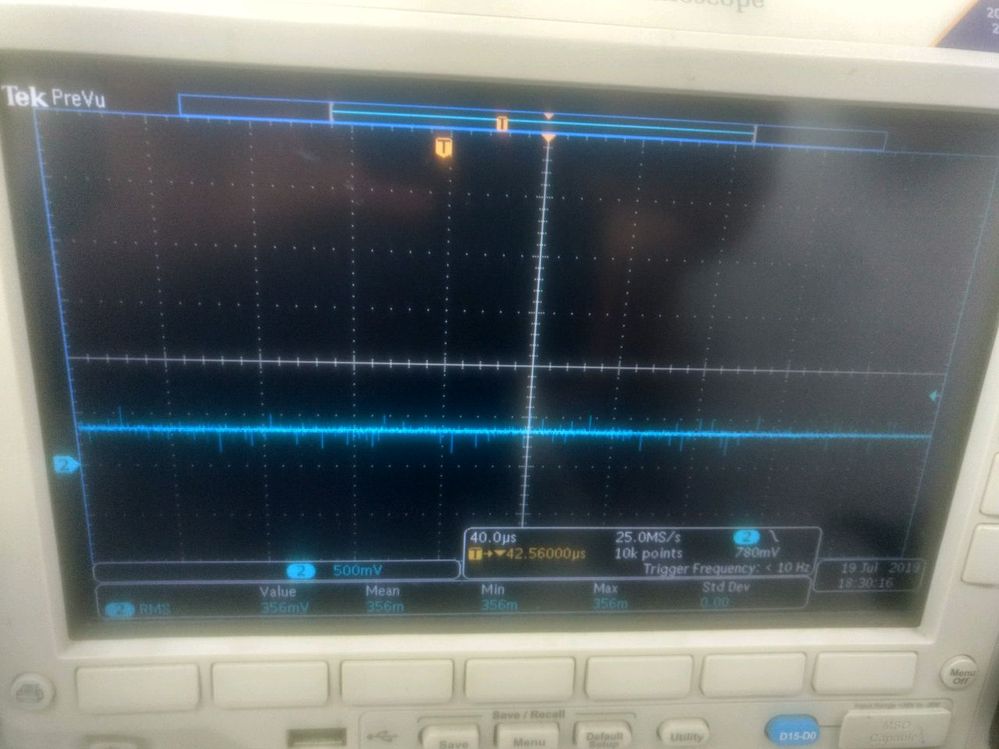
We are using PCA9509 chipset on my custom board. The VOL level of the chipset port A 3.5V.
As per datasheet page# 8, it should be 0.2V typical & <0.3V Max, If VCCA is >1.35V.
Our VCCA is 1.8V & VCCB is 3.3V.
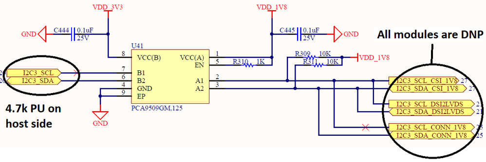
Find below schematic for your reference.
Following things tried:
1. Tried weak pullups. Changed 10k resistor to on U41 A1 port to 20k.
2. Check V input on U41 B1 port to ensure the VIL level match for B port. It is matching, the signal on port B reflects on port A.
Please advice the solution.
- Mark as New
- Bookmark
- Subscribe
- Mute
- Subscribe to RSS Feed
- Permalink
- Report Inappropriate Content
Hello Ritesh,
What do you have connected on the A side? If you present an issue in all the boards, it is possible that there is a hardware issue on what do you have connected to that side. Double checking the part of the schematic provided, it looks good.
The PCA9509 has a remark:
"Ground offset between the PCA9509 ground and the ground of devices on port A of the PCA9509 must be avoided. The reason for this cautionary remark is that a CMOS/NMOS open-drain capable of sinking 3 mA of current at 0.4 V has an output resistance of 133 or less (R = E / I). Such a driver shares enough current with the port A output pull-down of the PCA9509 to be seen as a LOW as long as the ground offset is zero. If the ground offset is greater than 0 V, then the driver resistance must be less. Since VILc can be as low as 90 mV at cold temperatures and the low end of the current distribution, the maximum ground offset should not exceed 50 mV. Bus repeaters that use an output offset are not interoperable with the port A of the PCA9509 as their output LOW levels will not be recognized by the PCA9509 as a LOW. If the PCA9509 is placed in an application where the VIL of port A of the PCA9509 does not go below its VILc, it pulls port B LOW initially when port A input transitions LOW, but the port B returns HIGH, so it does not reproduce the port A input on port B. Such applications should be avoided."
Have a great day,
Paulina
- Mark as New
- Bookmark
- Subscribe
- Mute
- Subscribe to RSS Feed
- Permalink
- Report Inappropriate Content
Hello Ritesh,
Have you tried the circuit shown in Fig 5 of the datasheet? Just some small changes. Each of the port A I/Os has an internal pull-up current source and does not require the external pull-up resistor but should not affect the system. Please try it and see how it works.
Another point is that, please keep in mind that the EN pin should change only in idle state to prevent system failures. Idle state is when the bus is not being used (when SDA and SCL are in High state).
Also, do you have another PCA9509 that can you swap for the one used? Just to make sure if can be a bad IC.
Have a great day,
Paulina.
- Mark as New
- Bookmark
- Subscribe
- Mute
- Subscribe to RSS Feed
- Permalink
- Report Inappropriate Content
Hi Paulina,
Thanks for the response.
1. We used the same circuit shown in the figure#5. We also tried by removing resistors on port A. There is no improvement.
2. We tied Enable pin with PCA chip power supply pin. So when power is applied, EN goes high & then after there is no any change in that.
3. We assembled 10 proto boards. We verified on 7 boards. All same results.
Please advice any other solution.
- Mark as New
- Bookmark
- Subscribe
- Mute
- Subscribe to RSS Feed
- Permalink
- Report Inappropriate Content
Hello Ritesh,
So, 3 out of the 10 boards are working as it should be, correct? If so, it is possible that this can be a quality issue with the ICs. In this case, you can submit a failure analysis request directly with the authorized distributor who sold you the parts and they will follow up properly.
Have a great day,
Paulina
- Mark as New
- Bookmark
- Subscribe
- Mute
- Subscribe to RSS Feed
- Permalink
- Report Inappropriate Content
Hi Paulina,
No. 3 boards out of 10 was not powered up yesterday. We tested those 3 boards as well & the issue is same.
I don't think this is the issue with IC now.

