- Forums
- Product Forums
- General Purpose MicrocontrollersGeneral Purpose Microcontrollers
- i.MX Forumsi.MX Forums
- QorIQ Processing PlatformsQorIQ Processing Platforms
- Identification and SecurityIdentification and Security
- Power ManagementPower Management
- Wireless ConnectivityWireless Connectivity
- RFID / NFCRFID / NFC
- Advanced AnalogAdvanced Analog
- MCX Microcontrollers
- S32G
- S32K
- S32V
- MPC5xxx
- Other NXP Products
- S12 / MagniV Microcontrollers
- Powertrain and Electrification Analog Drivers
- Sensors
- Vybrid Processors
- Digital Signal Controllers
- 8-bit Microcontrollers
- ColdFire/68K Microcontrollers and Processors
- PowerQUICC Processors
- OSBDM and TBDML
- S32M
- S32Z/E
-
- Solution Forums
- Software Forums
- MCUXpresso Software and ToolsMCUXpresso Software and Tools
- CodeWarriorCodeWarrior
- MQX Software SolutionsMQX Software Solutions
- Model-Based Design Toolbox (MBDT)Model-Based Design Toolbox (MBDT)
- FreeMASTER
- eIQ Machine Learning Software
- Embedded Software and Tools Clinic
- S32 SDK
- S32 Design Studio
- GUI Guider
- Zephyr Project
- Voice Technology
- Application Software Packs
- Secure Provisioning SDK (SPSDK)
- Processor Expert Software
- Generative AI & LLMs
-
- Topics
- Mobile Robotics - Drones and RoversMobile Robotics - Drones and Rovers
- NXP Training ContentNXP Training Content
- University ProgramsUniversity Programs
- Rapid IoT
- NXP Designs
- SafeAssure-Community
- OSS Security & Maintenance
- Using Our Community
-
- Cloud Lab Forums
-
- Knowledge Bases
- ARM Microcontrollers
- i.MX Processors
- Identification and Security
- Model-Based Design Toolbox (MBDT)
- QorIQ Processing Platforms
- S32 Automotive Processing Platform
- Wireless Connectivity
- CodeWarrior
- MCUXpresso Suite of Software and Tools
- MQX Software Solutions
- RFID / NFC
- Advanced Analog
-
- NXP Tech Blogs
- Home
- :
- Product Forums
- :
- OSBDM and TBDML
- :
- Programming JS16 with USBDM (JM)
Programming JS16 with USBDM (JM)
- Subscribe to RSS Feed
- Mark Topic as New
- Mark Topic as Read
- Float this Topic for Current User
- Bookmark
- Subscribe
- Mute
- Printer Friendly Page
Programming JS16 with USBDM (JM)
- Mark as New
- Bookmark
- Subscribe
- Mute
- Subscribe to RSS Feed
- Permalink
- Report Inappropriate Content
Hi!
This is a follow-up to my post from June https://community.nxp.com/message/669508
For bypassing the JS16 bootloader, it's important that the addresses FFB8/9/A are written:
FFB8: Flash Block Checksum High Byte
FFB9: Flash Block Checksum High Byte
FFBA: Checksum Bypass
It seems that the USBDM Flash Programmer does not write these.
E.g. this is the content of my s19 file:
S106FFB8D135003C
Written with USBDMs Flash Programmer and read again using USBDM Memory Dump, I get this:
S123FFA0FFFFFFFFFFFFFFFFFFFFFFFFFFFF01ADFFFFFFFFFFFFFFFFFFFFFFFFFFFFFFFEAE
Written with a PE Multilink:
S123FFA0FFFFFFFFFFFFFFFFFFFFFFFFFFFF01AEFFFFFFFFFFFFFFFFD13500FFFFFFFFFEA4
The difference AD vs AE is OK. This is the clock trim value.
The checksum is calculated from 0xC400 TO 0xFFAD and 0xFFC0 TO 0xFFFF so the trim value does not affect the checksum.
It seems that the USBDM programmer just ignores anything in this address range. Maybe the Flash Programmer is calculating the trim value and writing just this to this page.
Also, the "Verify Flash" does not find this difference.
Programmer: 4.12.1.140
BDM Firmware 4.12.1
DLL Ver 4.12.1.130
Windows 7 Professional, 64 bit
Regards,
Dietmar
- Mark as New
- Bookmark
- Subscribe
- Mute
- Subscribe to RSS Feed
- Permalink
- Report Inappropriate Content
Hi Peter,
thanks a lot. This works.
I would not expect that the Security setting does affect more than the two bits of 0xFFBF. There's no reason for that.
USBDM need not calculate checksums. These are in the s19 file and not affected from the contents of 0xFFAD to 0xFFC0.
It's controlled by the .prm file. E.g. for a JS16 it has these lines:
CHECKSUM
CHECKSUM_ENTRY
METHOD_CRC_CCITT
INIT 0x8D9D
OF READ_ONLY 0xC400 TO 0xFFAD
OF READ_ONLY 0xFFC0 TO 0xFFFF
INTO READ_ONLY 0xFFB8 SIZE 2
UNDEFINED 0xff
END
END
Regards,
Dietmar
- Mark as New
- Bookmark
- Subscribe
- Mute
- Subscribe to RSS Feed
- Permalink
- Report Inappropriate Content
Hi Dietmar,
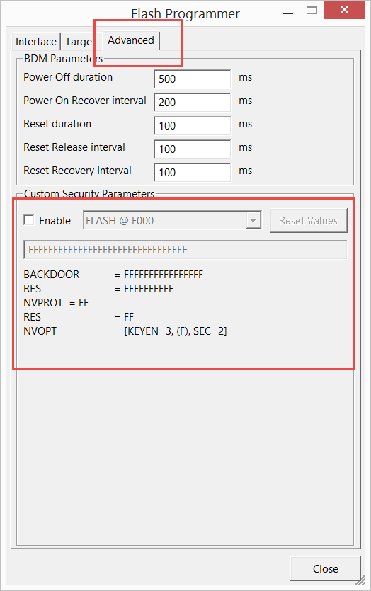
I view the 16 bytes including the the BACKDOOR key and such to be part of the same structure.
The following are clearly "security related"
BACKDOOR
FLASH/EEPROM protection
SECURITY byte.
The other data that has appeared in this area is less so.
When I originally wrote the programmer interface I thought it useful to have functionality to set the data for this area independent of the memory image. If I was doing it again I would probably be more minimalist. These days I usually map the whole area to a C struct and program it from the image.
Perhaps I should name it something else or change it but it's unlikely to happen.
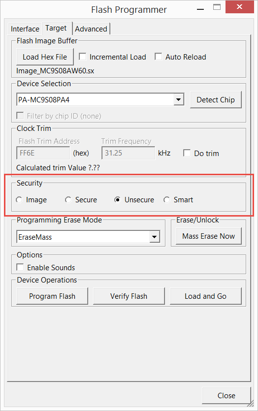
Note if you choose the "Smart" option then it should use the data from the image if present or use the programmer settings if not. This is the option I usually use.
bye
- Mark as New
- Bookmark
- Subscribe
- Mute
- Subscribe to RSS Feed
- Permalink
- Report Inappropriate Content
Hi Dietmar,
I'm sorry I missed your earlier post.
The security region of the flash is treated differently by the programmer.
Have a look at the advanced tab in the stand-alone programmer if you wish to manually set these values.
Alternatively, choose "Image" in the target tab to program as regular Flash.
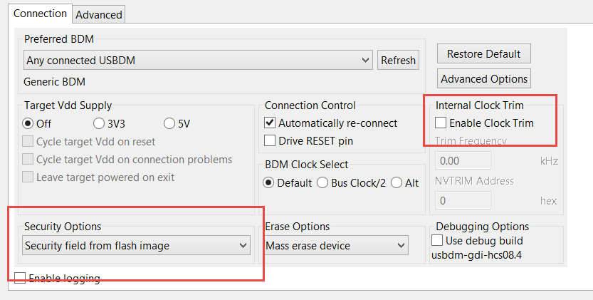
In Codewarrior these options are controlled by the launch configuration.
USBDM verifies the flash against these modified values. It does not ignore the differences.
USBDM does not support calculating flash checksums so this would have to be done in some other fashion.
bye


