- Forums
- Product Forums
- General Purpose MicrocontrollersGeneral Purpose Microcontrollers
- i.MX Forumsi.MX Forums
- QorIQ Processing PlatformsQorIQ Processing Platforms
- Identification and SecurityIdentification and Security
- Power ManagementPower Management
- Wireless ConnectivityWireless Connectivity
- RFID / NFCRFID / NFC
- Advanced AnalogAdvanced Analog
- MCX Microcontrollers
- S32G
- S32K
- S32V
- MPC5xxx
- Other NXP Products
- S12 / MagniV Microcontrollers
- Powertrain and Electrification Analog Drivers
- Sensors
- Vybrid Processors
- Digital Signal Controllers
- 8-bit Microcontrollers
- ColdFire/68K Microcontrollers and Processors
- PowerQUICC Processors
- OSBDM and TBDML
- S32M
- S32Z/E
-
- Solution Forums
- Software Forums
- MCUXpresso Software and ToolsMCUXpresso Software and Tools
- CodeWarriorCodeWarrior
- MQX Software SolutionsMQX Software Solutions
- Model-Based Design Toolbox (MBDT)Model-Based Design Toolbox (MBDT)
- FreeMASTER
- eIQ Machine Learning Software
- Embedded Software and Tools Clinic
- S32 SDK
- S32 Design Studio
- GUI Guider
- Zephyr Project
- Voice Technology
- Application Software Packs
- Secure Provisioning SDK (SPSDK)
- Processor Expert Software
- Generative AI & LLMs
-
- Topics
- Mobile Robotics - Drones and RoversMobile Robotics - Drones and Rovers
- NXP Training ContentNXP Training Content
- University ProgramsUniversity Programs
- Rapid IoT
- NXP Designs
- SafeAssure-Community
- OSS Security & Maintenance
- Using Our Community
-
- Cloud Lab Forums
-
- Knowledge Bases
- ARM Microcontrollers
- i.MX Processors
- Identification and Security
- Model-Based Design Toolbox (MBDT)
- QorIQ Processing Platforms
- S32 Automotive Processing Platform
- Wireless Connectivity
- CodeWarrior
- MCUXpresso Suite of Software and Tools
- MQX Software Solutions
- RFID / NFC
- Advanced Analog
-
- NXP Tech Blogs
- RSS フィードを購読する
- トピックを新着としてマーク
- トピックを既読としてマーク
- このトピックを現在のユーザーにフロートします
- ブックマーク
- 購読
- ミュート
- 印刷用ページ
K32L2A31VLL1A Schematic/Sample Design
- 新着としてマーク
- ブックマーク
- 購読
- ミュート
- RSS フィードを購読する
- ハイライト
- 印刷
- 不適切なコンテンツを報告
Hi,
I want to use the "K32L2A31VLL1A" MCU to develop the design for one of my products. I have gone through the below links.
1. K32L2A31VLL1A Product Information|NXP
I have gone with some of the documents and evaluation boards but I was not able to get the proper design for the MCU.
Can someone suggest if they have the design for this MCU?
Your support in this regard will be highly appreciable. And Thank you so much in Advance.
Regards
Kapil
- 新着としてマーク
- ブックマーク
- 購読
- ミュート
- RSS フィードを購読する
- ハイライト
- 印刷
- 不適切なコンテンツを報告
Hi Kapil Kesharvani,
The K32L2A31VLL1A related circuit can refer to the FRDM-K32L2A4S schematic directly.
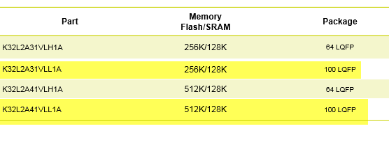
FRDM-K32L2A4S on board chip is K32L2A41VLL1A, your chip is K32L2A31VLL1A , even the package is the same, just the Flash and SRAM difference:
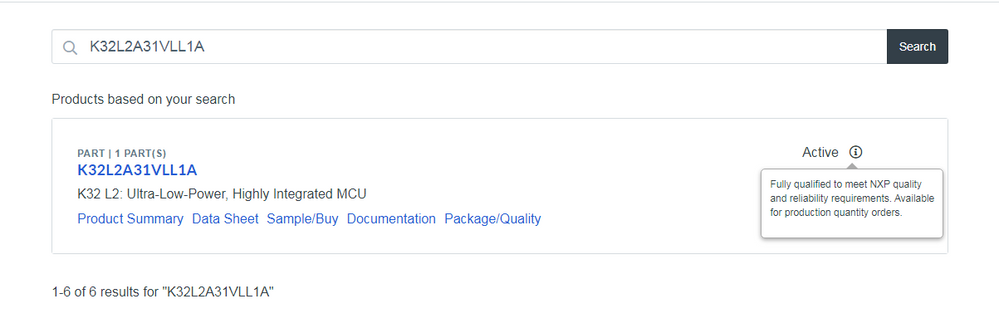
About the samples, you can apply it from the nxp.com:
You can find it is active now.
About the board, you can refer to the FRDM-K32L2A4S, you can use FRDM-K32L2A4S directly or change the on board chip to K32L2A31VLL1A.
About the peripheral hardware, the same as FRDM-K32L2A4S, you can refer to it directly.
1. SPI (1 no.)
2. I2C (1 no.)
3. UART(1 no.)
4. JTAG Debug
5. GPIOs, (30/40 numbers)
Check the fanout J1,J2, J3,J4 refer to your own design.
6. Clock, Reset, etc...
clock,
reset pin, 4.7K to 10K pullup, and 0.1uf capacitor to ground.
More details, check the FRDM schematic which I give you, you totally can refer to it.
Wish it helps you!
Kerry
-------------------------------------------------------------------------------
Note:
- If this post answers your question, please click the "Mark Correct" button. Thank you!
- We are following threads for 7 weeks after the last post, later replies are ignored
Please open a new thread and refer to the closed one, if you have a related question at a later point in time.
-------------------------------------------------------------------------------
- 新着としてマーク
- ブックマーク
- 購読
- ミュート
- RSS フィードを購読する
- ハイライト
- 印刷
- 不適切なコンテンツを報告
Hi Kapil Kesharvani,
Thanks for your interest in the NXP kinetis product, I would like to provide service for you.
K32L2A31VLL1A can refer to the FRDM-K32L2A4S:
FRDM-K32L2A4S Platform | Freedom Development Board | K32 L MCUs | NXP
But, it seems the design file still not put in the nxp website.
Anyway, I will help you to check it with our internal side,apply for upload the related schematic and the design file to the website.
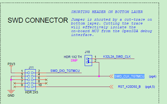
Here I share with you one K32L2A4 schematic at first.
Wish it helps you!
If you still have questions about it, please kindly let me know.
Kerry
-------------------------------------------------------------------------------
Note:
- If this post answers your question, please click the "Mark Correct" button. Thank you!
- We are following threads for 7 weeks after the last post, later replies are ignored
Please open a new thread and refer to the closed one, if you have a related question at a later point in time.
-------------------------------------------------------------------------------
- 新着としてマーク
- ブックマーク
- 購読
- ミュート
- RSS フィードを購読する
- ハイライト
- 印刷
- 不適切なコンテンツを報告
Hello Kerry,
Thank you so much for your reply.
Since we are going to finalize this MCU. So it is possible to share the sample design/ Application for the same MCU as soon as possible. And we need some samples and evaluation boards. so how soon we can get this?
As mentioned before, I am going through the datasheet and try to understand the features that we are looking for. But for better clarification can you suggest which pins are good for the below features.
The main features that we are going to use are:
1. SPI (1 no.)
2. I2C (1 no.)
3. UART(1 no.)
4. JTAG Debug
5. GPIOs, (30/40 numbers)
6. Clock, Reset, etc...
Regards
Kapil
- 新着としてマーク
- ブックマーク
- 購読
- ミュート
- RSS フィードを購読する
- ハイライト
- 印刷
- 不適切なコンテンツを報告
Hi Kerry,
I am sorry for the late reply. and thank you so much for your inputs.
Let me go through the inputs you shared. I will come back.
Regards
Kapil
- 新着としてマーク
- ブックマーク
- 購読
- ミュート
- RSS フィードを購読する
- ハイライト
- 印刷
- 不適切なコンテンツを報告
You are welcome!
If you have the question about this case, just let me know.
If you have the new questions, please create the new question post, thanks.
Kerry
-------------------------------------------------------------------------------
Note:
- If this post answers your question, please click the "Mark Correct" button. Thank you!
- We are following threads for 7 weeks after the last post, later replies are ignored
Please open a new thread and refer to the closed one, if you have a related question at a later point in time.
-------------------------------------------------------------------------------
- 新着としてマーク
- ブックマーク
- 購読
- ミュート
- RSS フィードを購読する
- ハイライト
- 印刷
- 不適切なコンテンツを報告
Hello Kerry,
Thank you so much for your reply.
Since we are going to finalize this MCU. So it is possible to share the sample design/ Application for the same MCU as soon as possible. And we need some samples and evaluation boards. so how soon we can get this?
As mentioned before, I am going through the datasheet and try to understand the features that we are looking for. But for better clarification can you suggest which pins are good for the below features.
The main features that we are going to use are:
1. SPI (1 no.)
2. I2C (1 no.)
3. UART(1 no.)
4. JTAG Debug
5. GPIOs, (30/40 numbers)
6. Clock, Reset, etc...
Regards
Kapil
- 新着としてマーク
- ブックマーク
- 購読
- ミュート
- RSS フィードを購読する
- ハイライト
- 印刷
- 不適切なコンテンツを報告
Hi Kapil Kesharvani ,
Please check the SDK code for FRDM-K32L2A4S from this link:
https://mcuxpresso.nxp.com/en/select
You will find all the related sample code for the perpherals.
Wish it helps you!
Kerry
-------------------------------------------------------------------------------
Note:
- If this post answers your question, please click the "Mark Correct" button. Thank you!
- We are following threads for 7 weeks after the last post, later replies are ignored
Please open a new thread and refer to the closed one, if you have a related question at a later point in time.
-------------------------------------------------------------------------------
- 新着としてマーク
- ブックマーク
- 購読
- ミュート
- RSS フィードを購読する
- ハイライト
- 印刷
- 不適切なコンテンツを報告
Hi Kerry,
Thanks for the reply. and sharing the inputs.
But my query was related to Schematic design.
it is possible to share the MCU (K32L2A31VLL1A) sample design (Circuit)/ Application design.
As mentioned before, I am going through the datasheet and try to understand the features that we are looking for. But for better clarification can you suggest which pins are good for the below features.
The main features that we are going to use are:
1. SPI (1 no.)
2. I2C (1 no.)
3. UART(1 no.)
4. JTAG Debug
5. GPIOs, (30/40 numbers)
6. Clock, Reset, etc...
And we need some samples and evaluation boards. what will be the lead time?
Regards
Kapil


