antenna design for sl3s1013ftb0.115
- 新着としてマーク
- ブックマーク
- 購読
- ミュート
- RSS フィードを購読する
- ハイライト
- 印刷
- 不適切なコンテンツを報告
For the NXP RFID chip sl3s1013ftb0.115, we think a largish, simple printed 1/4 wave dipole antenna, may give us better performance in the environment we use in our petroleum spill buckets, compared to the smaller coiled printed circuit antenna found in out existing smaller tags. In the application, we have a plastic collar around the gasoline filling pipe under the steel caps in the pavement at filling stations. Our system identifies the type of gasoline, via the tag, to prevent mis-fills. We thought an antenna geometry that maximized the antenna size to the 1/2 wavelength (about 6 " for 900 MHz), so that it can wrap at least half way around the pipe, would give it a better probability of capturing a mode, when the reader is placed on top of the bucket. We are having trouble with existing 'tags' in this application, that seem to encounter deep fades in the multipath environment down in the spill bucket. We have the luxury of some space, and wondered if a maximized antenna design is fairly straight forward.
What is the complex impedance of the antenna ports of the sl3s1013ftb0.115, such that a straight or slightly curved copper stripline extending out from both ends of the chip can be sized for max resonance etc?
Best Regards,
-John Fessler
CIVACON
Part of OPW (a Dover company)
- 新着としてマーク
- ブックマーク
- 購読
- ミュート
- RSS フィードを購読する
- ハイライト
- 印刷
- 不適切なコンテンツを報告
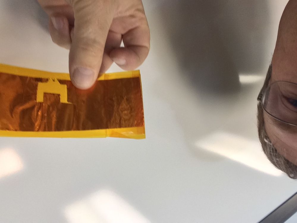
I cut out a rough version
of the Large Antenna Reference Design,
using capton tape and copper foil,
with #30AWG wire connections to chip
SL3S1013FTB0.115.
My colleague here has a regular ol' 800-900 MHz reader,
which reads our current RFID tags fine.
But we get no response from this first attempt.
Could you tell me what are the most common mistakes in this approach?
Should it read like a 'regular ol' RFID chip?
I'll check my solder connections.
Best Regards,
-John
- 新着としてマーク
- ブックマーク
- 購読
- ミュート
- RSS フィードを購読する
- ハイライト
- 印刷
- 不適切なコンテンツを報告
Oops, I did a poor job soldering on the first try.
After carefully soldering we get a fine reading.
Now off to optimizing the large antenna!
Thanks again for your support.
Best Regards,
-John
CIVACON EE
- 新着としてマーク
- ブックマーク
- 購読
- ミュート
- RSS フィードを購読する
- ハイライト
- 印刷
- 不適切なコンテンツを報告
The data sheet has: 2.2.2 Antenna design benefits High sensitivity enables small and cost efficient antenna designs Low Q-Value eases broad band antenna design for global usage
Visually unwinding the outer legs on a commercial tag I have here, gives this 2 x 3" long dipole sharing a loop coupler, as shown here with the sl3s1013ftb. But what would drive the geometry of the loop? I had heard that a high impedance is necessary for diode detected rf power to result a voltage of sufficient amplitude to rectify into a usable supply voltage inside the IC. Unfortunately, I have no rf simulator software to experiment, and wanted a good first guess for the PC board house.
Bset Regards,
Braden John Fessler
CIVACON EE
- 新着としてマーク
- ブックマーク
- 購読
- ミュート
- RSS フィードを購読する
- ハイライト
- 印刷
- 不適切なコンテンツを報告
Hello,
For the impedance, you can check the datasheet of the device on chapter 12. Characteristics.
And for that specific part, you can check the reference designs available UCODE G2i PCB Antenna Reference Designs with more details in the AN11215. Those are available in the Software and Tools tab UCODE G2iM and G2iM+|NXP in the part page.
Regards,
Estephania
- 新着としてマーク
- ブックマーク
- 購読
- ミュート
- RSS フィードを購読する
- ハイライト
- 印刷
- 不適切なコンテンツを報告
Excellent Estephania! I overlooked the impedance table in Section 12 on the data sheet. And together with the app note on antenna reference designs is just what I was looking for. Thank you.
Best Regards,
-John Fessler
CIVACON

