PN7160 EMI Problems
Hello NXP team,
We are using the PN7160 for the first time in 2 new designs.
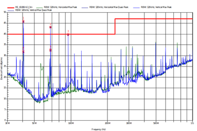
Functionality is very good, unfortunately the EMI measurements in both (different) designs show limit violations at 40.68MHz (3rd harmonics) by approx. 3-6dB, occasionally also 67.8MHz and 94.92MHz (5th, 7th harmonics). A (Desfire) card was placed during these tests so the app was in “presence check” mode.
What did we try?
* Reducing the power by reducing TXLDO to 2.7V (a quarter power)->
This only brought a small improvement, if any.
* EMI filter L0/C0 to 14.4MHz instead of 22MHz (without adjusting the rest, or values calculated with the tool) ->
This only brought a small improvement, if any, or in the higher frequency range.
TXLDO was set to 2V7, the DPC was not active/configured, current about 190mA.
* Place a series resistor (33R) between PN7160-TX1/TX2 and the inductors.
Brings improvements in the EMI, very bad functionality, is just nonsense.
What else could we try or check?
Is it possible to set the slope of TX1 and TX2 via the CLIF_ANA_TX_AMPLITUDE_REG as described in the RF settings guide?
Can you give me some values that I could try?
Can we reduce the power further by increasing the Z or is there something else to look for?
Are there any other software options for reducing the radiated power?
Our antenna (Rectangular):
64x38, 3 turns, Flex-PCB (with 40mm feed line, but that should work since we have already gotten other designs through EMI testing with this antenna).
Our matching:
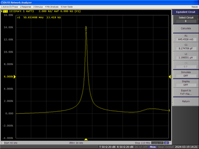
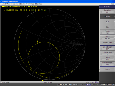
Asymmetrical matching, DPC not activated, Z = 24R
LQW18CNR16J0H 160nH / C0 = 330pF
C1 = 78p, C2 = 122p, Rq = 2R2
Our Config (see attachment):
# CFG2: VBAT2 to 3V9
NXP_EXT_TVDD_CFG_2={20, 02, 0F, 01, A0, 0E, 0B, 11, 01, 02, B2, 00, B2, 1E, 9F, 00, D0, 0C}
Measure Current Factoryapp: 5V: Idle: 155mA, with card: 83mA
Measure Current Factoryapp: 3V9 : Idle: 128mA, with card: 146mA (??)
Thanks and regards,
Michael
Hello Michael,
Have you already seen these two documents?
--> https://www.nxp.com/docs/en/application-note/AN13892.pdf --> 7 How to support/pass ETSI and FCC tests
--> https://www.nxp.com/docs/en/application-note/AN12988.pdf --> 11 Radiated Spurious Emissions
These two chapters could help.
However, I don´t think that we will fully solve the issue by reducing the output power by register settings.
Imagine that the drop of 3dB is 50% of the power.
- We need to check layout, especially the NFC part. Can you share the full design files, please? (Layout + schematic).
- Slightly increase the C0 capacitors to have more symmetrical tuning
- Do you have some EMI measurements without a DESfire card? Just RF ON or Polling ? It would be interesting to see the EMI radiation for nominal tuning.
About the layout. What is the loop I marked with green?
BR
Tomas
Hi Tomas,
I tested the whole thing without a card in the RF field via NfcFactoryApp PRBS / Type A / 106 kBit (or is there another way to switch to card polling with 100% duty cycle?).
The result is better here.
According to our findings, the whole thing depends not only on whether a card or token is in the field, but also on how it is positioned (orientation).
EMI filter L0/C0 to 14.4MHz instead of 22MHz (without adjusting the rest, or values calculated with the tool) -> This only brought a small improvement, if any, or in the higher frequency range.
Our idea was to be able to adjust the slope of TX1 and TX2 via a register. For example via the TX_GSN_CW_RM or TX_GSN_MOD_RM settings. If that makes any sense.
The marked loop is GND which was drawn manually because the layout flood engine does not fill everything here.
I will attach the layout data in our case.
The circuit diagram can also already be found there. (Please note that the “VNA-optimized” capacitor values are not yet entered in the circuit diagram)
If you need anything else let me know!
BR,
Michael
Measure NfcFactoryApp PRBS / Type A / 106 kBit / 2V7 / No Card
Hi michael_d_1983,
We created a case about your issue. Can you confirm that you have access there, please?
BR
Tomas


