
- Forums
- Product Forums
- General Purpose MicrocontrollersGeneral Purpose Microcontrollers
- i.MX Forumsi.MX Forums
- QorIQ Processing PlatformsQorIQ Processing Platforms
- Identification and SecurityIdentification and Security
- Power ManagementPower Management
- Wireless ConnectivityWireless Connectivity
- RFID / NFCRFID / NFC
- Advanced AnalogAdvanced Analog
- Neural Processing UnitsNeural Processing Units
- MCX Microcontrollers
- S32G
- S32K
- S32V
- MPC5xxx
- Other NXP Products
- S12 / MagniV Microcontrollers
- Powertrain and Electrification Analog Drivers
- Sensors
- Vybrid Processors
- Digital Signal Controllers
- 8-bit Microcontrollers
- ColdFire/68K Microcontrollers and Processors
- PowerQUICC Processors
- OSBDM and TBDML
- S32M
- S32Z/E
-
- Solution Forums
- Software Forums
- MCUXpresso Software and ToolsMCUXpresso Software and Tools
- CodeWarriorCodeWarrior
- MQX Software SolutionsMQX Software Solutions
- Model-Based Design Toolbox (MBDT)Model-Based Design Toolbox (MBDT)
- FreeMASTER
- eIQ Machine Learning Software
- Embedded Software and Tools Clinic
- S32 SDK
- S32 Design Studio
- GUI Guider
- Zephyr Project
- Voice Technology
- Application Software Packs
- Secure Provisioning SDK (SPSDK)
- Processor Expert Software
- Generative AI & LLMs
-
- Topics
- Mobile Robotics - Drones and RoversMobile Robotics - Drones and Rovers
- NXP Training ContentNXP Training Content
- University ProgramsUniversity Programs
- Rapid IoT
- NXP Designs
- SafeAssure-Community
- OSS Security & Maintenance
- Using Our Community
-
- Cloud Lab Forums
-
- Knowledge Bases
- ARM Microcontrollers
- i.MX Processors
- Identification and Security
- Model-Based Design Toolbox (MBDT)
- QorIQ Processing Platforms
- S32 Automotive Processing Platform
- Wireless Connectivity
- CodeWarrior
- MCUXpresso Suite of Software and Tools
- MQX Software Solutions
- RFID / NFC
- Advanced Analog
- Neural Processing Units
-
- NXP Tech Blogs
- Home
- :
- Translated Content
- :
- Multi Source Translation Content
- :
- 2082914_en-US
2082914_en-US
2082914_en-US
2082914_en-US
Hi NXP team,
We are currently using S32K144 and have encountered a problem. Could you please help us solve it? Thanks!
From S32K1xx_Memory_Map.xlsx of the RM, the start address of SRAM_U is 0x2000_0000:
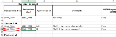
Could m_data_2‘s ORIGIN in the link file S32K144_64_flash.ld of S32K144 be set arbitrarily? For example, can it be changed to be less than 0x2000_0000 as following?
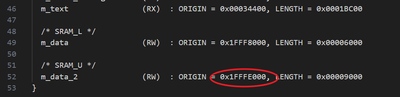
BTW, we made an initial attempt(change m_data_2‘s ORIGIN to 0x1FFFE000) and confirmed that the compilation could be successfully passed in the S32DS environment, and the generated program could be smoothly downloaded to the S32K144 product board with a normal running status.
Thanks,
Alex
Hi Senlent,
OK got it, thanks a lot.
Thanks,
Alex
Hi@AlexKlose
There will be no error if you define it this way, and there will be no error if you download it to MCU.
What I want to tell you is that we have some considerations when designing the link file in this way, and it is allocated according to SRAM_L and SRAM_U.
Whether there are potential problems when you modify the link file in this way, you need to do sufficient testing yourself.
Hi Senlent,
Sorry, I still don't quite understand what you meant in the last post...
I merely want to make sure whether this operation(m_data_2‘s ORIGIN to 0x1FFFE000) itself is legal or not. If not, we would try to optimize the code to reduce the size of the .bss section.
Thanks,
Alex
Hi@AlexKlose
Usually users may not pay attention to the fact that SRAM_L and SRAM_U are two different blocks.
This needs to be noted when dealing with certain issues, such as ECC processing.

Hi Senlent,
Thanks for your quick response.
Since SRAM_L and SRAM_U are two separate physical RAMs, is this operation (m_data_2‘s ORIGIN to 0x1FFFE000) compliant? What risks does it entail?
"which is more reasonable, but you will not get an error if you define it this way." That means we can still do it this way to expand the space of m_data_2 although this operation is not recommended?
Thanks,
Alex
Hi@AlexKlose
The reason why we define it this way is based on the physical address space of the two blocks of SRAM, which is more reasonable, but you will not get an error if you define it this way.
For s32k144,
the SRAM_L address range is :0x1FFF8000~0x1FFFFFFF
the SRAM_U address range is: 0x20000000~0x20006FFF

0x1FFFE000 is in the range SRAM_L, but it is not SRAM_U.