
- Forums
- Product Forums
- General Purpose MicrocontrollersGeneral Purpose Microcontrollers
- i.MX Forumsi.MX Forums
- QorIQ Processing PlatformsQorIQ Processing Platforms
- Identification and SecurityIdentification and Security
- Power ManagementPower Management
- Wireless ConnectivityWireless Connectivity
- RFID / NFCRFID / NFC
- Advanced AnalogAdvanced Analog
- Neural Processing UnitsNeural Processing Units
- MCX Microcontrollers
- S32G
- S32K
- S32V
- MPC5xxx
- Other NXP Products
- S12 / MagniV Microcontrollers
- Powertrain and Electrification Analog Drivers
- Sensors
- Vybrid Processors
- Digital Signal Controllers
- 8-bit Microcontrollers
- ColdFire/68K Microcontrollers and Processors
- PowerQUICC Processors
- OSBDM and TBDML
- S32M
- S32Z/E
-
- Solution Forums
- Software Forums
- MCUXpresso Software and ToolsMCUXpresso Software and Tools
- CodeWarriorCodeWarrior
- MQX Software SolutionsMQX Software Solutions
- Model-Based Design Toolbox (MBDT)Model-Based Design Toolbox (MBDT)
- FreeMASTER
- eIQ Machine Learning Software
- Embedded Software and Tools Clinic
- S32 SDK
- S32 Design Studio
- GUI Guider
- Zephyr Project
- Voice Technology
- Application Software Packs
- Secure Provisioning SDK (SPSDK)
- Processor Expert Software
- Generative AI & LLMs
-
- Topics
- Mobile Robotics - Drones and RoversMobile Robotics - Drones and Rovers
- NXP Training ContentNXP Training Content
- University ProgramsUniversity Programs
- Rapid IoT
- NXP Designs
- SafeAssure-Community
- OSS Security & Maintenance
- Using Our Community
-
- Cloud Lab Forums
-
- Knowledge Bases
- ARM Microcontrollers
- i.MX Processors
- Identification and Security
- Model-Based Design Toolbox (MBDT)
- QorIQ Processing Platforms
- S32 Automotive Processing Platform
- Wireless Connectivity
- CodeWarrior
- MCUXpresso Suite of Software and Tools
- MQX Software Solutions
- RFID / NFC
- Advanced Analog
- Neural Processing Units
-
- NXP Tech Blogs
- Home
- :
- Translated Content
- :
- Multi Source Translation Content
- :
- 2023071_en-US
2023071_en-US
- Subscribe to RSS Feed
- Mark as New
- Mark as Read
- Bookmark
- Subscribe
- Printer Friendly Page
- Report Inappropriate Content
2023071_en-US
2023071_en-US
Dear Team,
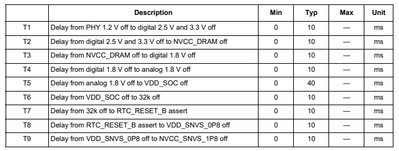
We have observed that some power-down timing results do not meet the SoC's requirements. According to the specification, the power-down timing range must be between 0 and 10 ms. However, our measurement results did not meet this specification.
As far as I know, the power-down behavior will depend on the capacitor value and loading on the PCBA, which may explain why the timing range specified in the document cannot be met by all products. Would a failure in power-down timing have any impact on the product? Could we ignore the failures?
Here are the test results.
T1. Delay from PHY 1.2 V off to digital 2.5 V and 3.3 V off, the test results are -0.43ms~-0.3ms.
T3. Delay from NVCC_DRAM off to digital 1.8 V off, the test results are -0.18ms~-0.14ms.
T4. Delay from digital 1.8 V off to analog 1.8 V off, the test results are -0.31ms~-0.19ms.
T5. Delay from analog 1.8 V off to VDD_SOC off, the test results are -34.9us~-31.1us.
T9. Delay from VDD_SNVS_0P8 off to NVCC_SNVS_1P8 off, the test results are -3.97us~-2.53us.

Please provide recommendations.
The understanding of the customer is correct. If PCA9450 is used for i.MX8MN application, the measurement result should be fine because all power rails will be discharged completely by the PMIC.
I will confirm it .
Hi Rita,
This is the data measured on our design.
Will there be any risks if we cannot meet the power-down requirement?
Which board are you using? NXP reference board or the board you design yourself?