- Forums
- Product Forums
- General Purpose MicrocontrollersGeneral Purpose Microcontrollers
- i.MX Forumsi.MX Forums
- QorIQ Processing PlatformsQorIQ Processing Platforms
- Identification and SecurityIdentification and Security
- Power ManagementPower Management
- Wireless ConnectivityWireless Connectivity
- RFID / NFCRFID / NFC
- Advanced AnalogAdvanced Analog
- MCX Microcontrollers
- S32G
- S32K
- S32V
- MPC5xxx
- Other NXP Products
- S12 / MagniV Microcontrollers
- Powertrain and Electrification Analog Drivers
- Sensors
- Vybrid Processors
- Digital Signal Controllers
- 8-bit Microcontrollers
- ColdFire/68K Microcontrollers and Processors
- PowerQUICC Processors
- OSBDM and TBDML
- S32M
- S32Z/E
-
- Solution Forums
- Software Forums
- MCUXpresso Software and ToolsMCUXpresso Software and Tools
- CodeWarriorCodeWarrior
- MQX Software SolutionsMQX Software Solutions
- Model-Based Design Toolbox (MBDT)Model-Based Design Toolbox (MBDT)
- FreeMASTER
- eIQ Machine Learning Software
- Embedded Software and Tools Clinic
- S32 SDK
- S32 Design Studio
- GUI Guider
- Zephyr Project
- Voice Technology
- Application Software Packs
- Secure Provisioning SDK (SPSDK)
- Processor Expert Software
- Generative AI & LLMs
-
- Topics
- Mobile Robotics - Drones and RoversMobile Robotics - Drones and Rovers
- NXP Training ContentNXP Training Content
- University ProgramsUniversity Programs
- Rapid IoT
- NXP Designs
- SafeAssure-Community
- OSS Security & Maintenance
- Using Our Community
-
- Cloud Lab Forums
-
- Knowledge Bases
- ARM Microcontrollers
- i.MX Processors
- Identification and Security
- Model-Based Design Toolbox (MBDT)
- QorIQ Processing Platforms
- S32 Automotive Processing Platform
- Wireless Connectivity
- CodeWarrior
- MCUXpresso Suite of Software and Tools
- MQX Software Solutions
- RFID / NFC
- Advanced Analog
-
- NXP Tech Blogs
- Home
- :
- QorIQプロセッシングプラットフォーム
- :
- レイヤースケープ
- :
- Re: MC34VR500 new configuration
MC34VR500 new configuration
- RSS フィードを購読する
- トピックを新着としてマーク
- トピックを既読としてマーク
- このトピックを現在のユーザーにフロートします
- ブックマーク
- 購読
- ミュート
- 印刷用ページ
MC34VR500 new configuration
- 新着としてマーク
- ブックマーク
- 購読
- ミュート
- RSS フィードを購読する
- ハイライト
- 印刷
- 不適切なコンテンツを報告
Hello all,
I used the 34VR500 (V1) as PMIC for my LS1 design which worked so far really well.
Now we faced an issue during the really early boot-up of the module and I tried to adjust the sequencing of the PMIC to get rid of the issue. Long story short I'm not able to program the internal RAM of the PMIC.
Question #1:
Why is the internal user space carry out as RAM? This makes it necessary to write the new setup every time after a rest ... that's true?
Question #2:
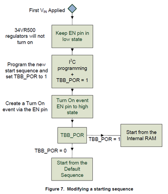
How it should work? In Figure 7 of the datasheet, you can see that the programming needs to be done before the enable pin becomes a release. So how this should work? If the PMIC isn't alive the LS1 isn't alive too, how should program the PMIC ... a second controller?
Question #3:
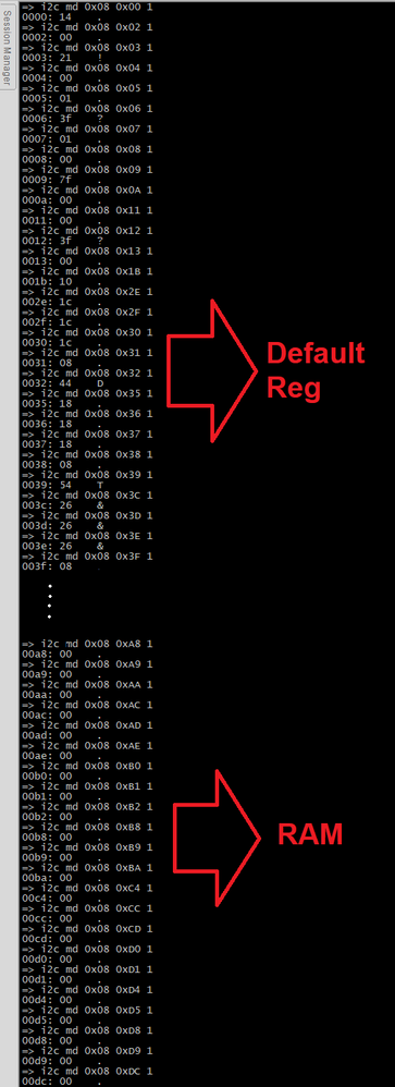
I got the feedback from EBV that there isn't s Spezial sequencing needed and it would be possible to write to the internal RAM at any time. I tried it in different configurations and I never was able to read any value back from the internal RAM.
Question #4:
The description of the internal RAM register is really poor, is there a detailed description available?
Best regards and thank you in advance
Ch. Sielaff
- 新着としてマーク
- ブックマーク
- 購読
- ミュート
- RSS フィードを購読する
- ハイライト
- 印刷
- 不適切なコンテンツを報告
Thank you for feedback. Let I reword my answer
A1) I think they supposed that one selects suitable chip from the MC34VR500xxx family and needs for dynamic control via I2C only. And the factheet says: "* Dynamic regulator control of voltage, current limit, and frequency via I2C".
A2 - If the powered chip cannot start with preprogrammed configuration then it is supposed that system has external controller which can configure the MC34VR500xxx properly.
May be I wrong - there is no official document which explain why "RAM". What is your suggestion? By the way I agree with you that nonvolatile R/W registers will be better.
A3) Have you observed output changing after writing to the control register? I do not see how you write to the registers. Please check if you have the same problem like in https://community.nxp.com/t5/Power-Management/Register-settings-for-MC34VR500V1/m-p/999191#M719
A4) Could you please create a technical case with that questions? It is definitely should be sent to the factory experts.
Best regards,
Serguei
- 新着としてマーク
- ブックマーク
- 購読
- ミュート
- RSS フィードを購読する
- ハイライト
- 印刷
- 不適切なコンテンツを報告
Ans.4) The internal RAM registers are described in the MC34VR500, Multi-output DC/DC Regulator for LS1/T1 Family of Communications Processors Data Sheet
https://www.nxp.com/docs/en/data-sheet/MC34VR500.pdf
Notice it was updated a week ago.
Ans.1) The datasheet says directly: “The 34VR500 starts up from the internal configuration, which is hard-coded into the device. However, the 34VR500 can be controlled through the I2C port after the Start-up sequence. It is also possible to modify the contents of the Internal Registers via the bus I2C to modify the start up parameters”. It also shows that there are 12 hard-corded configurations (see Table 8. Start-up configuration). On page https://www.nxp.com/products/power-management/pmics-and-sbcs/pmics/multi-output-dc-dc-regulator:MC34... one can select right PMIC for used MPU.
There were one time programmable VR5100 see application note https://www.nxp.com/docs/en/application-note/AN5403.pdf
Ans.2) Obviously powered device which cannot accept the hard-coded configuration cannot reprogram it.
Ans.3) If is not clear what do you mean as any time and different configurations. Please while PMIC is in the ON state try to read ID register to check your I2C communications.
- 新着としてマーク
- ブックマーク
- 購読
- ミュート
- RSS フィードを購読する
- ハイライト
- 印刷
- 不適切なコンテンツを報告
Hello r8070z,
thanks for your answer.
To question #1:
My first questions were why the user configuration space where carry out as RAM? I know that the 34VR500 are available in 12 different pre-configured versions that's not the question. The PMIC has the possibility to adjust the sequencing ... but if this user adjustment is stored in a volatile memory what benefit I can gain here for my design?
To question #2:
So this means the feature is unusable ... or? Because if powered device which cannot accept the hard-coded configuration cannot reprogram it. An unpowered device that accepts the configuration can reprogram it or what? What's the use case here?
To question #3:
I can read all the registers of the PMIC even when I keep them at rest. So the I2C communication works fine. But it does not matter what I write in the RAM area I always read 0x00 back.
To question #4:
Thanks for the latest version of the datasheet but even in this version the RAM registers are poorly described! For example, I can't find the description of Reg 0xE0 - "PU CONFIG1" or reg 0xE8 - "PWRGD EN". That's unacceptable for a datasheet in revision 12.
Best regards and thank you in advance
Christian


