- Forums
- Product Forums
- General Purpose MicrocontrollersGeneral Purpose Microcontrollers
- i.MX Forumsi.MX Forums
- QorIQ Processing PlatformsQorIQ Processing Platforms
- Identification and SecurityIdentification and Security
- Power ManagementPower Management
- Wireless ConnectivityWireless Connectivity
- RFID / NFCRFID / NFC
- Advanced AnalogAdvanced Analog
- MCX Microcontrollers
- S32G
- S32K
- S32V
- MPC5xxx
- Other NXP Products
- S12 / MagniV Microcontrollers
- Powertrain and Electrification Analog Drivers
- Sensors
- Vybrid Processors
- Digital Signal Controllers
- 8-bit Microcontrollers
- ColdFire/68K Microcontrollers and Processors
- PowerQUICC Processors
- OSBDM and TBDML
- S32M
- S32Z/E
-
- Solution Forums
- Software Forums
- MCUXpresso Software and ToolsMCUXpresso Software and Tools
- CodeWarriorCodeWarrior
- MQX Software SolutionsMQX Software Solutions
- Model-Based Design Toolbox (MBDT)Model-Based Design Toolbox (MBDT)
- FreeMASTER
- eIQ Machine Learning Software
- Embedded Software and Tools Clinic
- S32 SDK
- S32 Design Studio
- GUI Guider
- Zephyr Project
- Voice Technology
- Application Software Packs
- Secure Provisioning SDK (SPSDK)
- Processor Expert Software
- Generative AI & LLMs
-
- Topics
- Mobile Robotics - Drones and RoversMobile Robotics - Drones and Rovers
- NXP Training ContentNXP Training Content
- University ProgramsUniversity Programs
- Rapid IoT
- NXP Designs
- SafeAssure-Community
- OSS Security & Maintenance
- Using Our Community
-
- Cloud Lab Forums
-
- Knowledge Bases
- ARM Microcontrollers
- i.MX Processors
- Identification and Security
- Model-Based Design Toolbox (MBDT)
- QorIQ Processing Platforms
- S32 Automotive Processing Platform
- Wireless Connectivity
- CodeWarrior
- MCUXpresso Suite of Software and Tools
- MQX Software Solutions
- RFID / NFC
- Advanced Analog
-
- NXP Tech Blogs
- Home
- :
- General Purpose Microcontrollers
- :
- LPC Microcontrollers
- :
- SDRAM Reference code for Understanding the functionality
SDRAM Reference code for Understanding the functionality
- Subscribe to RSS Feed
- Mark Topic as New
- Mark Topic as Read
- Float this Topic for Current User
- Bookmark
- Subscribe
- Mute
- Printer Friendly Page
SDRAM Reference code for Understanding the functionality
- Mark as New
- Bookmark
- Subscribe
- Mute
- Subscribe to RSS Feed
- Permalink
- Report Inappropriate Content
Hi Jeremy,
I am using LPC4367 controller with MCU Xpresso 10.3.0_2200. I am using SDRAM and NOR Flash interface in one of our projects. I was working with Evaluation board OM13088 but it that board no SDRAM and NOR flash interface is avialable. I am using SDRAM and NOR flash both interfaced with EMC lines aviable in LPC4367 controller.
I refered the code in e lpcopen_3_02_lpcxpresso_mcb4357 and also refered periph_memtest and misc_spifi_tst demos. But there is no EMC init routine avialable. Is there any sample code or a reference code for SDRAM with proper intitiatilization routine.
Also i want to allocate one of my Buffer to SDRAM address, i got the information related to it i MCU expresso User guied but still i want to know than as we user
__At(Address) attribute in Keil to allocate the array or a buffer like
uint16_t Buffer[1024] __at(0x28000000)
In the similar manner how we can use it in MCU Expresso . I have downloaded MCUxpresso 10.3.0 .
To conclude i want the sample or areference code for SDRAM and NOR flash with proper EMC init routine which not provided in existing reference code
I need this since i want to test my development board which is ready. So please consider it on higher priority. Mean while i am trying to refere other forums as well for my understanding.
Thanks
Gaurav More
- Mark as New
- Bookmark
- Subscribe
- Mute
- Subscribe to RSS Feed
- Permalink
- Report Inappropriate Content
Hi Jeremy,
Thank you very much for the consistent support from your side reagrding the SDRAM interface issue.
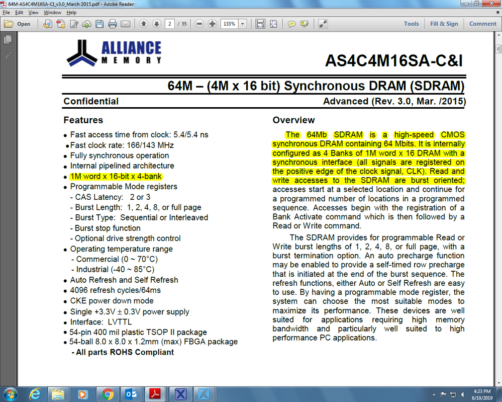
I am able to interface AS4C4M16SA-C&I" 64M – (4M x 16 bit) Synchronous DRAM (SDRAM) with LPC4367. I have tried a lot but after going going through the application note AN11508 and under standing the behaviour and conection required for interface i made some modifcation in the code which is mentioned below.
the major modification which enable me to interface SDRAM and access it properly is making the feedback clock conficguration for both the clock pin in case of LPC4367 as per the application note. In other controllers loke LPC546xx there is a provision for configuring the feed back clock source which is also mentioned in the data in basic configuration information whihc is missing in case of LPC43XX i guess.
/* SDRAM_CLK0 (EMC_CLK0)*/
Chip_SCU_ClockPinMuxSet(0, ( SCU_MODE_INACT | SCU_MODE_ZIF_DIS | SCU_MODE_INBUFF_EN | SCU_MODE_HIGHSPEEDSLEW_EN | SCU_MODE_FUNC5));
/* SDRAM_CLK2 (EMC_CLK3)*/
Chip_SCU_ClockPinMuxSet(2, ( SCU_MODE_INACT | SCU_MODE_ZIF_DIS | SCU_MODE_INBUFF_EN | SCU_MODE_HIGHSPEEDSLEW_EN | SCU_MODE_FUNC5));
This information is no where mentioned in the datasheet or user manual of LPC4367. This was the inout which i got from application not.
I am wondering how come your code is functional with the previous project which you share? Sicne after this modifcation only iwas able to access and read write the memory. I also checked with other SDRAM chip MT48LC16M16A2_TIG
Also reagarding the configureation i need to do some small modifications mentioned below
static const IP_EMC_DYN_CONFIG_T AS4C4M16SA_CI_Config ={
EMC_NANOSECOND(64000000 / 4096), /* Row refresh time (RefreshPeriod)*/
0x01, /* Dynamic Memory Read Configuration*/
EMC_NANOSECOND(18), /*< Precharge Command Period */
EMC_NANOSECOND(42), /*< Active to Precharge Command Period */
EMC_NANOSECOND(70), /*!< Self Refresh Exit Time */
EMC_CLOCK(1), /*!< Last Data Out to Active Time */
EMC_CLOCK(5), /*!< Data In to Active Command Time */
EMC_NANOSECOND(12), /*!< Write Recovery Time */
EMC_NANOSECOND(60), /*!< Active to Active Command Period */
EMC_NANOSECOND(60), /*!< Auto-refresh Period */
EMC_NANOSECOND(70), /*!< Exit Self Refresh */
EMC_NANOSECOND(12), /*!< Active Bank A to Active Bank B Time */
EMC_CLOCK(2), /*!< Load Mode register command to Active Command */
{
{
/*!< Device Configuration array with SDRAM Mode register*/
EMC_ADDRESS_DYCS0, /* Base Register*/
3, /* RAS */
/* Mode Register value*/
EMC_DYN_MODE_WBMODE_PROGRAMMED |
EMC_DYN_MODE_OPMODE_STANDARD |
EMC_DYN_MODE_CAS_3 |
EMC_DYN_MODE_BURST_TYPE_SEQUENTIAL |
EMC_DYN_MODE_BURST_LEN_8,
/* Device Config [0]*/
EMC_DYN_CONFIG_DATA_BUS_16 |
EMC_DYN_CONFIG_LPSDRAM |
EMC_DYN_CONFIG_4Mx16_4BANKS_12ROWS_8COLS |
EMC_DYN_CONFIG_MD_SDRAM
},
{0, 0, 0, 0}, /* Device Config [1]*/
{0, 0, 0, 0}, /* Device Config [2]*/
{0, 0, 0, 0} /* Device Config [3]*/
}
};
After doing the modification mentioned above in bold and changing the configurations i an able to verify the SDRAM code.
But still will again confirm after i redesign the development board with proper cconnection. Hope it shpild work there as well since it s working with 20Mhz frequency above which it is not working. I guess there is routing iissue as per the application note which we need to redesign as per the instrcutio mentioned in the Applicaton note.
Thanks
Gaurav More
- Mark as New
- Bookmark
- Subscribe
- Mute
- Subscribe to RSS Feed
- Permalink
- Report Inappropriate Content
Hi Gaurav More,
Thanks for your reply.
According to the AN11508, the clock configuration supports two kinds of modes, and they are select freely the developer.
For the MCB4357 board, it uses the EMC_CLK0 to drive the SDRAM MT48LC4M32B2P when the EMC_CLK0 pin works as the function 0, in addition, the EMC_FBCLK0 feature is enabled too.
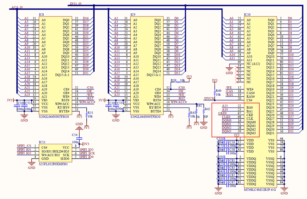
I've attached the schematic about the MT48LC4M32B2P connection, and the related demo project, please refer to it for details.
Have a great day,
TIC
-------------------------------------------------------------------------------
Note:
- If this post answers your question, please click the "Mark Correct" button. Thank you!
- We are following threads for 7 weeks after the last post, later replies are ignored
Please open a new thread and refer to the closed one, if you have a related question at a later point in time.
-------------------------------------------------------------------------------
- Mark as New
- Bookmark
- Subscribe
- Mute
- Subscribe to RSS Feed
- Permalink
- Report Inappropriate Content
Hi Jeremy,
Thanks for the reply.
I am not able to identify the code section where EMC_FBCLK0 is enabled in the code that you shared. However now ai am able to access the SDRAM since that was feature whcih was not enabled in my code whcih i was able to make out by going through app note AN11508.
Thanks
Gaurav More
- Mark as New
- Bookmark
- Subscribe
- Mute
- Subscribe to RSS Feed
- Permalink
- Report Inappropriate Content
Hi Gaurav More,
Thanks for your reply.
1) I am not able to identify the code section where EMC_FBCLK0 is enabled in the code that you shared.
-- Please check the below figure.
Have a great day,
TIC
-------------------------------------------------------------------------------
Note:
- If this post answers your question, please click the "Mark Correct" button. Thank you!
- We are following threads for 7 weeks after the last post, later replies are ignored
Please open a new thread and refer to the closed one, if you have a related question at a later point in time.
-------------------------------------------------------------------------------
- Mark as New
- Bookmark
- Subscribe
- Mute
- Subscribe to RSS Feed
- Permalink
- Report Inappropriate Content
Hi Jeremy,
Thanks for the reply.
But if you see, the clock muxing array consist of
STATIC const PINMUX_GRP_T pinclockmuxing[] = {
{0, 0, (SCU_MODE_INACT | SCU_MODE_INBUFF_EN | SCU_MODE_ZIF_DIS | SCU_MODE_HIGHSPEEDSLEW_EN | SCU_MODE_FUNC0)},
{0, 1, (SCU_MODE_INACT | SCU_MODE_INBUFF_EN | SCU_MODE_ZIF_DIS | SCU_MODE_HIGHSPEEDSLEW_EN | SCU_MODE_FUNC0)},
{0, 2, (SCU_MODE_INACT | SCU_MODE_INBUFF_EN | SCU_MODE_ZIF_DIS | SCU_MODE_HIGHSPEEDSLEW_EN | SCU_MODE_FUNC0)},
{0, 3, (SCU_MODE_INACT | SCU_MODE_INBUFF_EN | SCU_MODE_ZIF_DIS | SCU_MODE_HIGHSPEEDSLEW_EN | SCU_MODE_FUNC0)},
};
Where as the below mentioned modification is not reflected which I did for LPC4367 controller.
/* SDRAM_CLK0 (EMC_CLK0)*/
Chip_SCU_ClockPinMuxSet(0, ( SCU_MODE_INACT | SCU_MODE_ZIF_DIS | SCU_MODE_INBUFF_EN | SCU_MODE_HIGHSPEEDSLEW_EN | SCU_MODE_FUNC5));
/* SDRAM_CLK2 (EMC_CLK3)*/
Chip_SCU_ClockPinMuxSet(2, ( SCU_MODE_INACT | SCU_MODE_ZIF_DIS | SCU_MODE_INBUFF_EN | SCU_MODE_HIGHSPEEDSLEW_EN | SCU_MODE_FUNC5));
Thanks
Gaurav More
- Mark as New
- Bookmark
- Subscribe
- Mute
- Subscribe to RSS Feed
- Permalink
- Report Inappropriate Content
Hi Gaurav More
Thanks for your reply.
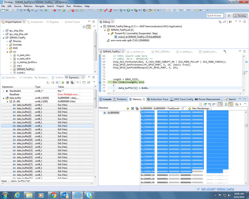
I've done some testing with your code in the periph_memtest demo, however, in debug, I don't encounter the similar phenomenon you mentioned before,
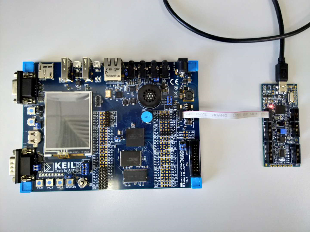
My board is MCB4357, IDE: LPCXpresso v8.2.2.
Fig 1
Fig 2
Have a great day,
TIC
-------------------------------------------------------------------------------
Note:
- If this post answers your question, please click the "Mark Correct" button. Thank you!
- We are following threads for 7 weeks after the last post, later replies are ignored
Please open a new thread and refer to the closed one, if you have a related question at a later point in time.
-------------------------------------------------------------------------------
- Mark as New
- Bookmark
- Subscribe
- Mute
- Subscribe to RSS Feed
- Permalink
- Report Inappropriate Content
Hi Jeremy,
Looking at your code it works fine.
Do you find any discripency in the code that I am using compared to the code that you verified?
Is there any dependency of Debugger CMSIS-DAP LPClink2 or Jlink ?
Other wise my project should work fine as well.
Thanks
Gaurav More
- Mark as New
- Bookmark
- Subscribe
- Mute
- Subscribe to RSS Feed
- Permalink
- Report Inappropriate Content
Hi Gaurav More
Thanks for your reply.
1) Do you find any discrepancy in the code that I am using compared to the code that you verified?
-- In the periph_memtest demo, it would initialize the EMC prior to jumping to the main(), maybe you can give a try.
Q2) Is there any dependency of Debugger CMSIS-DAP LPClink2 or Jlink?
-- No, I don't think so, I also use the CMSIS-DAP debugger.
Have a great day,
TIC
-------------------------------------------------------------------------------
Note:
- If this post answers your question, please click the "Mark Correct" button. Thank you!
- We are following threads for 7 weeks after the last post, later replies are ignored
Please open a new thread and refer to the closed one, if you have a related question at a later point in time.
-------------------------------------------------------------------------------
- Mark as New
- Bookmark
- Subscribe
- Mute
- Subscribe to RSS Feed
- Permalink
- Report Inappropriate Content
Hi Jeremy,
Can you please share the code that you tested with MCB4357 board. I will check at my end for it functionality.
Thanks
Gaurav More
- Mark as New
- Bookmark
- Subscribe
- Mute
- Subscribe to RSS Feed
- Permalink
- Report Inappropriate Content
Hi Gaurav More
Thanks for your reply.
Please check the attachment.
Have a great day,
TIC
-------------------------------------------------------------------------------
Note:
- If this post answers your question, please click the "Mark Correct" button. Thank you!
- We are following threads for 7 weeks after the last post, later replies are ignored
Please open a new thread and refer to the closed one, if you have a related question at a later point in time.
-------------------------------------------------------------------------------
- Mark as New
- Bookmark
- Subscribe
- Mute
- Subscribe to RSS Feed
- Permalink
- Report Inappropriate Content
Hi Jeremy,
I check with my code for SDRAM and while running the code I found the following behaviour,
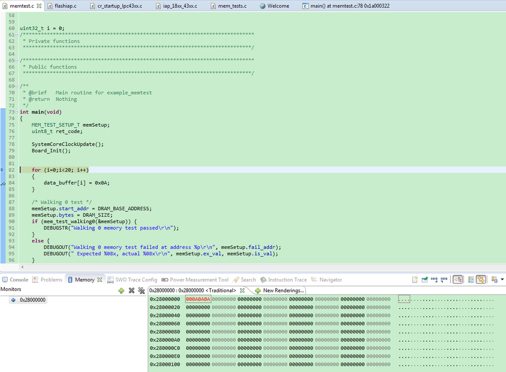
While loading the code and running the code it is observed that it is storing the data on multiple location.When I am running the code mentioned below with stepwise execution,
__SECTION(data,RAM8) uint8_t data_buffer[1024];
Length = DRAM_SIZE;
for (i=0;i<Length; i++)
{
data_buffer[i] = 0x0A;
}
I just run for i=0 and data_buffer[i] = 0x0A;
and then checked the memory. So follwing is the observation.
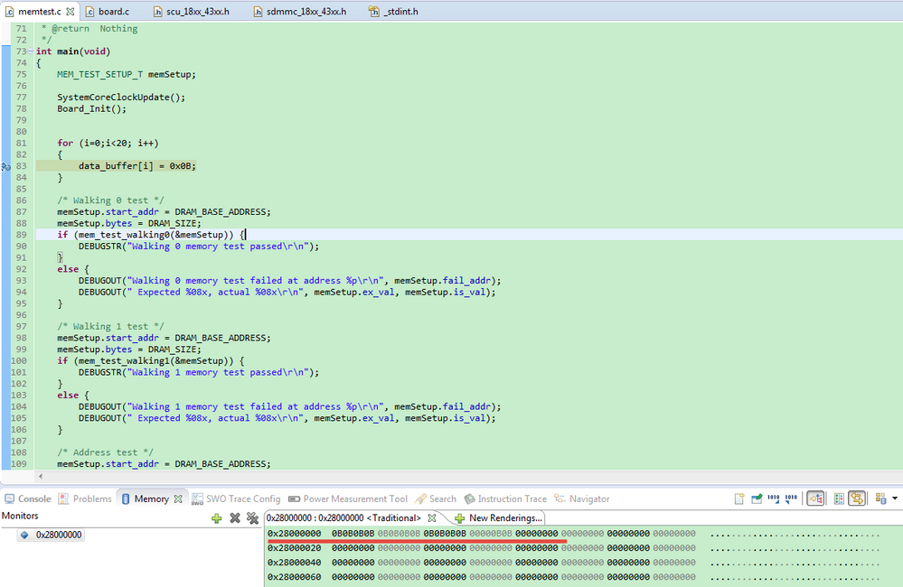
Instead of storing the data in only data_buffer[0] = 0x0A; sinze i=0 it is also storing the same value 0x0a in other locations as well refer the screen shot for observation.
Also one more observation is when I am stopping the execution stepwise and checking the data in expression and memory as shown below then again while proceeding for the next step then it gives below error
But if without the checking the debug value and running step by step the it works but it is storing the value in all other locations as well as i have mentione above.
Also I would like to suggest you to please check my code with your board by doing the modifications in the code w.r.t your eval board and check the behaviour. mean while i will check for the clock and other issues if exist.
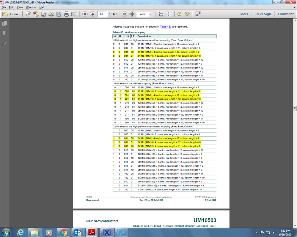
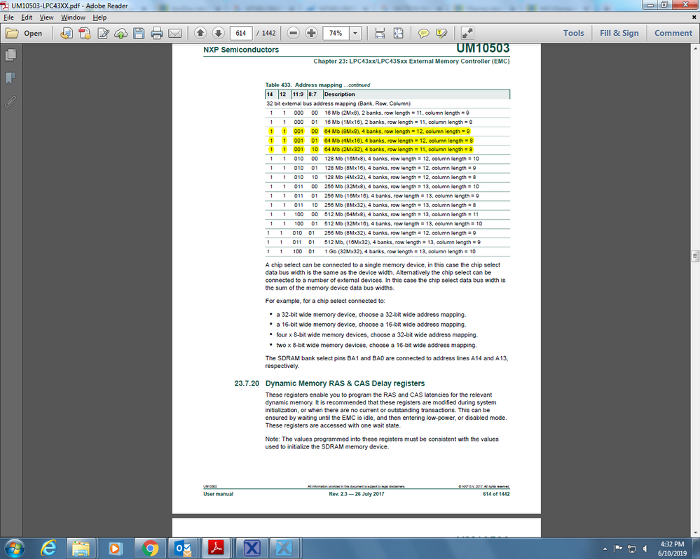
There is one more observation reagrding the memory that we are using.
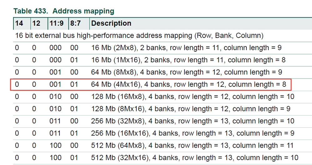
You can see highlighted part where is it mentioned the memory configuration. But similar memory configuration is not available in the user manual of LPC43XX.
is there a probelma related to this? Since the same behaviour is ther there after doing following method.
for (index = 0; index < 20; index++)
{
*(uint32_t *)(sdram + index) = 0xA5A5A5A5;
}
while(1)
{
Chip_GPIO_SetPinToggle(LPC_GPIO_PORT, 5, 19);
for (index=0; index<0xFFFFF;index++ );
//sdram = (uint32_t *)EMC_ADDRESS_DYCS0;
for (index = 0; index < 20; index++)
{
if (*(uint32_t *)(sdram + index) != 0xA5A5A5A5)
{
Chip_GPIO_SetPinState(LPC_GPIO_PORT, 5, 19, (bool) true);
while(1);
}
}
}
Here also it it writing the whole memory with 0xA5A5A5A5 instead of only 20 locations.
Also refer the attached code as well for your reference where I have made the modifications regarding your inputs as well.
Thanks
Gaurav More
- Mark as New
- Bookmark
- Subscribe
- Mute
- Subscribe to RSS Feed
- Permalink
- Report Inappropriate Content
Hi Gaurav More
Thanks for your reply.
Q1) I've not encountered a similar phenomenon as you mentioned when using below code
__SECTION(data,RAM8) uint8_t data_buffer[1024];
Length = DRAM_SIZE;
for (i=0;i<Length; i++)
{
data_buffer[i] = 0x0A;
}
Q2) The highlight configuration is suited for the AS4C4M16SA.
Q3) I've not encountered a similar phenomenon when using the below code.
for (index = 0; index < 20; index++)
{
*(uint32_t *)(sdram + index) = 0xA5A5A5A5;
}
while(1)
{
Chip_GPIO_SetPinToggle(LPC_GPIO_PORT, 5, 19);
for (index=0; index<0xFFFFF;index++ );
//sdram = (uint32_t *)EMC_ADDRESS_DYCS0;
for (index = 0; index < 20; index++)
{
if (*(uint32_t *)(sdram + index) != 0xA5A5A5A5)
{
Chip_GPIO_SetPinState(LPC_GPIO_PORT, 5, 19, (bool) true);
while(1);
}
}
}Note: I've done the above testing base on MCB4357 board, the demo code is based on the periph_memtest demo which is come from the LPCOpen library.
Have a great day,
TIC
-------------------------------------------------------------------------------
Note:
- If this post answers your question, please click the "Mark Correct" button. Thank you!
- We are following threads for 7 weeks after the last post, later replies are ignored
Please open a new thread and refer to the closed one, if you have a related question at a later point in time.
-------------------------------------------------------------------------------
- Mark as New
- Bookmark
- Subscribe
- Mute
- Subscribe to RSS Feed
- Permalink
- Report Inappropriate Content
Hi Jeremy,
Any update regarding the issue ir reported and also with respect to the forum i referred related to LQFP packages of LPC43XX since i am also using the same package for LPC4367.
https://community.nxp.com/thread/432972
Need input from the your side.
Thanks
Gaurav More
- Mark as New
- Bookmark
- Subscribe
- Mute
- Subscribe to RSS Feed
- Permalink
- Report Inappropriate Content
Hi Jeremy,
As per your input I the modifications in the code and also refered the application note (ANN11508) for SDRAM interface with LPC43XX.
After doing the modification I am able to write but the data written at the alternate address is not proper means not the one which want to write.
Let explian in detail. I am writing
uint16_t Data = 0xA5A5;
uint16_t Data1 = 0x1234;
In alternate location. and I am writting data using following logic,
for (index = 0; index < SDRAM_SIZE; index++)
{
if(Flag == 0 )
{
sdramAddr = Data;
*(sdram + index) = sdramAddr;
Flag = 1;
}
else
{
sdramAddr = Data1;
*(sdram + index) = sdramAddr;
Flag = 0;
}
if(*(sdram + index) != sdramAddr )
{
while(1);
}
}
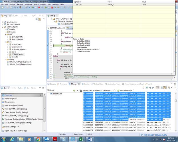
after cehcking the memory location 0x28000000, below is the observation where it is writing 0x1200 instead of 0x1234 and it is happening only for every alternate address address writing. it is writing 0xA5A5 properly.
It is storing 0xA5A5 at 0x28000000, 0x1200 at 0x28000002.. Likewise..
You can see it is writing 0x1200 and 0xA5A5 at every alternate location instead of writing 0x1234 and 0xA5A5.
Please let me know the reason for the same. Also find attached code for your reference. in order to check if any configuration is missing.
Thanks
Gaurav More
- Mark as New
- Bookmark
- Subscribe
- Mute
- Subscribe to RSS Feed
- Permalink
- Report Inappropriate Content
Hi Gaurav More,
Comparing with the previous project, I find that there's no
difference to initializing the SDRAM except for the CLK0's configuration.
However, it doesn't matter actually. And maybe you can tell me if I miss something.
About the new testing, I've migrated to the memtest demo to test, and it works well on the MCB4357 board.
Have a great day,
TIC
-------------------------------------------------------------------------------
Note:
- If this post answers your question, please click the "Mark Correct" button. Thank you!
- We are following threads for 7 weeks after the last post, later replies are ignored
Please open a new thread and refer to the closed one, if you have a related question at a later point in time.
-------------------------------------------------------------------------------
- Mark as New
- Bookmark
- Subscribe
- Mute
- Subscribe to RSS Feed
- Permalink
- Report Inappropriate Content
Hi Jeremy,
There is one observation in the functionality of SDRAM interfaced with LPC4367 in my customized board.
The observation is in the below mentioned code while writing the data
uint16_t Data = 0xA5A5;
uint16_t Data1 = 0x1234;
In alternate location. and I am writting data using following logic,
for (index = 0; index < SDRAM_SIZE; index++)
{
if(Flag == 0 )
{
sdramAddr = Data;
*(sdram + index) = sdramAddr;
Flag = 1;
}
else
{
sdramAddr = Data1;
*(sdram + index) = sdramAddr;
Flag = 0;
}
if(*(sdram + index) != sdramAddr )
{
while(1);
}
}
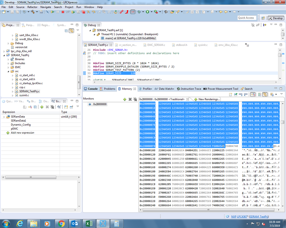
when #define SDRAM_SIZE 128
It works fine and writes proper in all the location. So as per my understanding I am able to write 0x28000000 to 0x28000100 means upto 256 bytes.
Patern mentioned below,
Address Data
0x28000000 0xA5A5
0x28000002 0x1234
0x28000004 0xA5A5
0x28000006 0x1234
like wise till 0x28000100 Which is correct one.
.
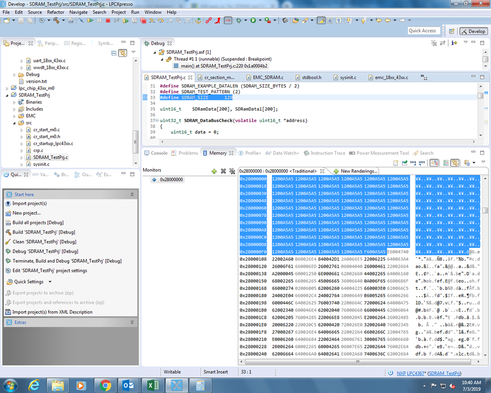
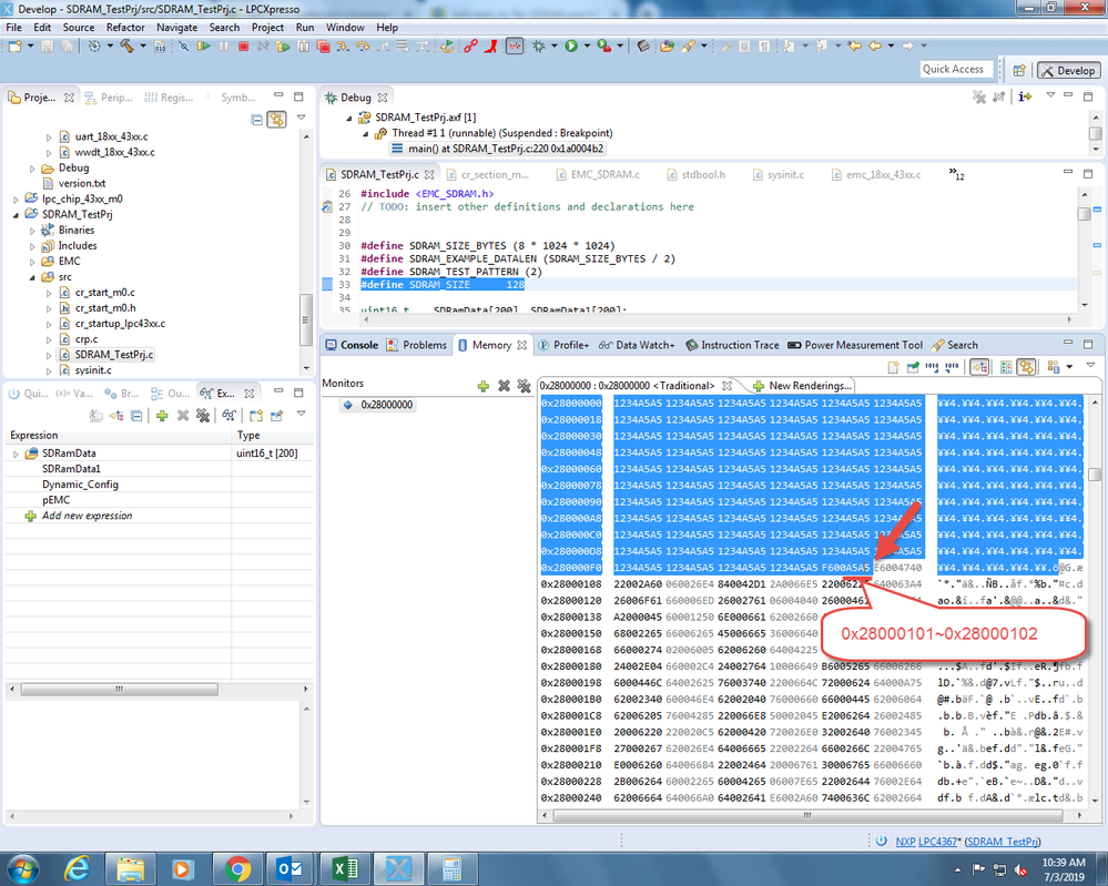
when #define SDRAM_SIZE 129
Above 0x28000100 means if address location is 0x28000102, it writes 0x1200 and it also corrupts the previous location as well, means from 0x28000000 to 0x28000100 address location by writing 0x1200 in every alternate location.
Patern mentioned below,
Address Data
0x28000000 0xA5A5
0x28000002 0x1200
0x28000004 0xA5A5
0x28000006 0x1200
like wise till 0x28000102 which is not correct.
Please let me know the reason for this behaviour mentioned above on very higher priority. IS there any thing missing in the code which is not allowing to write above 0x28000100 address location?
Thanks
Gaurav More.
- Mark as New
- Bookmark
- Subscribe
- Mute
- Subscribe to RSS Feed
- Permalink
- Report Inappropriate Content
Hi Gaurav More,
Sorry for reply late.
If the SDRAM_SIZE becomes 129, it means that the writing byte will be 258 bytes which consist of 0x2800101 and 0x2800102(will be written: 0xA5A5) and the previous 256 bytes.
So it's correct.
Have a great day,
TIC
-------------------------------------------------------------------------------
Note:
- If this post answers your question, please click the "Mark Correct" button. Thank you!
- We are following threads for 7 weeks after the last post, later replies are ignored
Please open a new thread and refer to the closed one, if you have a related question at a later point in time.
-------------------------------------------------------------------------------
- Mark as New
- Bookmark
- Subscribe
- Mute
- Subscribe to RSS Feed
- Permalink
- Report Inappropriate Content
Hi Jeremy,
Thanks for the reply.
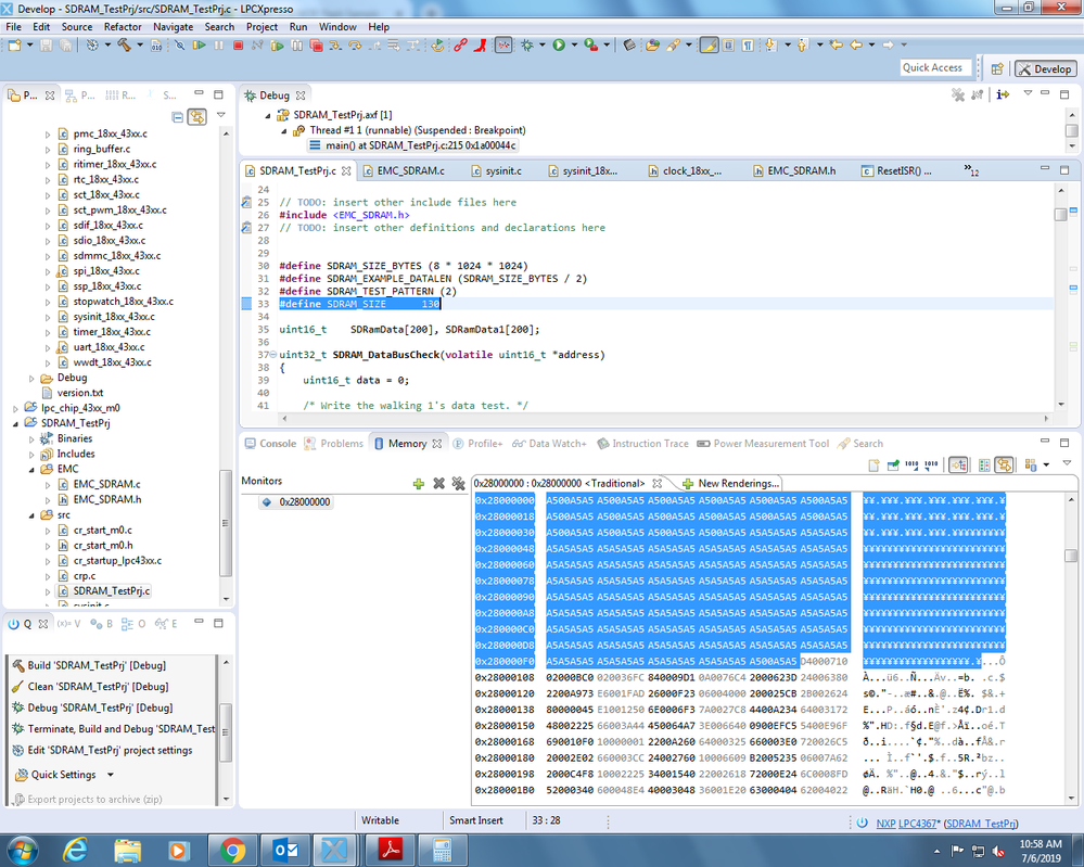
As per you input i did some more test to checl the behaviour. I made some modification in the code mentioned below and checked the behaviour
volatile uint16_t *sdram = (uint16_t *)EMC_ADDRESS_DYCS0; /* SDRAM start address. */
uint16_t sdramAddr;
uint16_t Data = 0xA5A5;
SDRAM_SIZE = 130;
for (index = 0; index < (SDRAM_SIZE); index ++)
{
sdramAddr = Data;
*(sdram + index) = sdramAddr;
}
And after running the code below is the result that i got whihc is different. I just wanted to check if i write the same data accross al location what is the output? Some plase it is writing properly and at some places it is writing 0xA500 instead of 0xA5A5.
You can see that it is writing randomly. Now I tried with the EMCCLK Delay 6 and 7 as well but still the same result.
What is the resaons please let me know..
Even i tried
memset((uint16_t *)sdram, 0xA5A5, 130);
but still the same result. It is not writing the data consistently.
I feel I am close to the solution but then again not getting the result.
Thanks
Gaurav More
- Mark as New
- Bookmark
- Subscribe
- Mute
- Subscribe to RSS Feed
- Permalink
- Report Inappropriate Content
Hi Gaurav More,
Thanks for your reply.
Please give a try with the address boundary is 32-bit aligned (that is
address bits [1:0] equal 0).
Have a great day,
TIC
-------------------------------------------------------------------------------
Note:
- If this post answers your question, please click the "Mark Correct" button. Thank you!
- We are following threads for 7 weeks after the last post, later replies are ignored
Please open a new thread and refer to the closed one, if you have a related question at a later point in time.
-------------------------------------------------------------------------------
- Mark as New
- Bookmark
- Subscribe
- Mute
- Subscribe to RSS Feed
- Permalink
- Report Inappropriate Content
Hi Jeremy,
Thanks for the reply.
You mean to say making the device 32 bit and then check. It so then i did that already but the same result. If not please explain what needs to be tested.
Also i am attaching the vedio where i did the testing and I recoded the behaviour which you can see and comments on it .
I kept the previous code as it is before making 32bit change and the first tested that. The behavious is as follow in breif.
I and writing 0xA5A5 in debugign mode step by step.
But when i write the first address it writes properly and when i write for the second address then also it writed properly. but in debuging as run the for loop you can see the secodong address which was 0xA5A5, gets changed in 0xA500. and this happens continuosly.
Kinldy go through the Video.
Thanks
Gaurav More
