- Forums
- Product Forums
- General Purpose MicrocontrollersGeneral Purpose Microcontrollers
- i.MX Forumsi.MX Forums
- QorIQ Processing PlatformsQorIQ Processing Platforms
- Identification and SecurityIdentification and Security
- Power ManagementPower Management
- Wireless ConnectivityWireless Connectivity
- RFID / NFCRFID / NFC
- Advanced AnalogAdvanced Analog
- MCX Microcontrollers
- S32G
- S32K
- S32V
- MPC5xxx
- Other NXP Products
- S12 / MagniV Microcontrollers
- Powertrain and Electrification Analog Drivers
- Sensors
- Vybrid Processors
- Digital Signal Controllers
- 8-bit Microcontrollers
- ColdFire/68K Microcontrollers and Processors
- PowerQUICC Processors
- OSBDM and TBDML
- S32M
- S32Z/E
-
- Solution Forums
- Software Forums
- MCUXpresso Software and ToolsMCUXpresso Software and Tools
- CodeWarriorCodeWarrior
- MQX Software SolutionsMQX Software Solutions
- Model-Based Design Toolbox (MBDT)Model-Based Design Toolbox (MBDT)
- FreeMASTER
- eIQ Machine Learning Software
- Embedded Software and Tools Clinic
- S32 SDK
- S32 Design Studio
- GUI Guider
- Zephyr Project
- Voice Technology
- Application Software Packs
- Secure Provisioning SDK (SPSDK)
- Processor Expert Software
- Generative AI & LLMs
-
- Topics
- Mobile Robotics - Drones and RoversMobile Robotics - Drones and Rovers
- NXP Training ContentNXP Training Content
- University ProgramsUniversity Programs
- Rapid IoT
- NXP Designs
- SafeAssure-Community
- OSS Security & Maintenance
- Using Our Community
-
- Cloud Lab Forums
-
- Knowledge Bases
- ARM Microcontrollers
- i.MX Processors
- Identification and Security
- Model-Based Design Toolbox (MBDT)
- QorIQ Processing Platforms
- S32 Automotive Processing Platform
- Wireless Connectivity
- CodeWarrior
- MCUXpresso Suite of Software and Tools
- MQX Software Solutions
- RFID / NFC
- Advanced Analog
-
- NXP Tech Blogs
Pinout and debugger configuration for reliable SWD on LPC810?
I want to explore the micro trace buffer on the 8-pin DIP LPC810 using the Keil uVision5 toolchain and a ULINK2 debugger. I've looked at the schematic for the LPC800 mini kit and also looked at other LPC810-based schematics by Leon Heller and Jim Eli in order to establish the correct wiring of the LPC's debug pins to the SWD connector.
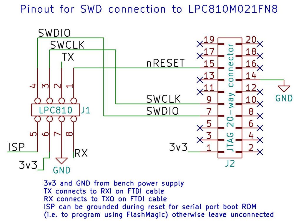
I have 3 wires connected from the LPC810 to the SWD connector: nRESET, SWCLK and SWDIO. I also have a common ground between them.
I created a simple program to re-enable the SWD and RESET pins via the switch matrix:
LPC_SWM->PINENABLE0 = 0xffffffb3;
I succesfully programmed the resultant .hex file using FlashMagic and was then able to get the Keil toolchain past the flash uploader stage and into debug mode. However, I don't appear to be able to set breakpoints, inspect memory or single-step.
Can anyone share their successful LPC810 SWD debug setup or does everyone use FlashMagic :smileyhappy: ?
Jim shared his code so I now have:
SYSCON_SYSAHBCLKCTRL |= (1<<7); // bit 7 for Switch Matrix (SWM) clock
LPC_SWM->PINENABLE0 = 0xffffffb3UL;
And the wiring that I have on my breadboard looks like
The above configuration works for Keil uVision 5.21a and a ULINK2 with the latest firmware
