- Forums
- Product Forums
- General Purpose MicrocontrollersGeneral Purpose Microcontrollers
- i.MX Forumsi.MX Forums
- QorIQ Processing PlatformsQorIQ Processing Platforms
- Identification and SecurityIdentification and Security
- Power ManagementPower Management
- Wireless ConnectivityWireless Connectivity
- RFID / NFCRFID / NFC
- Advanced AnalogAdvanced Analog
- MCX Microcontrollers
- S32G
- S32K
- S32V
- MPC5xxx
- Other NXP Products
- S12 / MagniV Microcontrollers
- Powertrain and Electrification Analog Drivers
- Sensors
- Vybrid Processors
- Digital Signal Controllers
- 8-bit Microcontrollers
- ColdFire/68K Microcontrollers and Processors
- PowerQUICC Processors
- OSBDM and TBDML
- S32M
- S32Z/E
-
- Solution Forums
- Software Forums
- MCUXpresso Software and ToolsMCUXpresso Software and Tools
- CodeWarriorCodeWarrior
- MQX Software SolutionsMQX Software Solutions
- Model-Based Design Toolbox (MBDT)Model-Based Design Toolbox (MBDT)
- FreeMASTER
- eIQ Machine Learning Software
- Embedded Software and Tools Clinic
- S32 SDK
- S32 Design Studio
- GUI Guider
- Zephyr Project
- Voice Technology
- Application Software Packs
- Secure Provisioning SDK (SPSDK)
- Processor Expert Software
- Generative AI & LLMs
-
- Topics
- Mobile Robotics - Drones and RoversMobile Robotics - Drones and Rovers
- NXP Training ContentNXP Training Content
- University ProgramsUniversity Programs
- Rapid IoT
- NXP Designs
- SafeAssure-Community
- OSS Security & Maintenance
- Using Our Community
-
- Cloud Lab Forums
-
- Knowledge Bases
- ARM Microcontrollers
- i.MX Processors
- Identification and Security
- Model-Based Design Toolbox (MBDT)
- QorIQ Processing Platforms
- S32 Automotive Processing Platform
- Wireless Connectivity
- CodeWarrior
- MCUXpresso Suite of Software and Tools
- MQX Software Solutions
- RFID / NFC
- Advanced Analog
-
- NXP Tech Blogs
- Home
- :
- General Purpose Microcontrollers
- :
- LPC Microcontrollers
- :
- LPC5516 ADC INPUT
LPC5516 ADC INPUT
- Subscribe to RSS Feed
- Mark Topic as New
- Mark Topic as Read
- Float this Topic for Current User
- Bookmark
- Subscribe
- Mute
- Printer Friendly Page
- Mark as New
- Bookmark
- Subscribe
- Mute
- Subscribe to RSS Feed
- Permalink
- Report Inappropriate Content
How many volts can the internal clamping diode of the LPC5516 clamp to? If the ADC input pin voltage is -0.4V, will it affect other MCU pins?
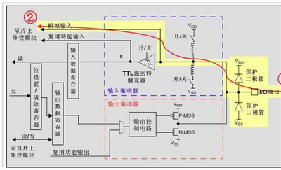
I found the following pictures from the Internet. Is the GPIO architecture of LPC5516 the same? I read that the LPC5516 manual states that the minimum analog input voltage is -0.3V. Will there be any impact if it exceeds it?
Solved! Go to Solution.
- Mark as New
- Bookmark
- Subscribe
- Mute
- Subscribe to RSS Feed
- Permalink
- Report Inappropriate Content
Extrapolating from other vendors/MCUs, about 0.6V.
However, not only does exceeding the max ratings reduce the lifetime, transverse currents through the clamping diodes will affect other ADC inputs, and most probably also other peripheral units.
I would suggest to avoid overvoltages, using proper external protection.
- Mark as New
- Bookmark
- Subscribe
- Mute
- Subscribe to RSS Feed
- Permalink
- Report Inappropriate Content
Hi, WeiQian,
Unfortunately, we do not provide the analog channel internal architecture for the LPC55xx family.
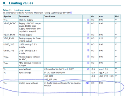
Regarding the analog channel voltage range for LPC55xx family, pls refer to the VIA specs in data sheet of LPC551x.
The limiting analog ADC voltage is from -0.3V to 3.96V, the normal analog ADC voltage is from 0V to VDDA.
If your ADC analog voltage is out of the range from -0.3 to 3.96V, external diodes are required to protect ADC.
Hope it can help you
BR
XiangJun Rong
I copy the notes here from the Data sheet.
[6] An ADC input voltage above 3.6 V can be applied for a short time without leading to immediate, unrecoverable failure. Accumulated
exposure to elevated voltages at 4.6 V must be less than 106 s total over the lifetime of the device. Applying an elevated voltage to the
ADC inputs for a long time affects the reliability of the device and reduces its lifetime.
[7] It is recommended to connect an overvoltage protection diode between the analog input pin and the voltage supply pin.

