- Forums
- Product Forums
- General Purpose MicrocontrollersGeneral Purpose Microcontrollers
- i.MX Forumsi.MX Forums
- QorIQ Processing PlatformsQorIQ Processing Platforms
- Identification and SecurityIdentification and Security
- Power ManagementPower Management
- MCX Microcontrollers
- S32G
- S32K
- S32V
- MPC5xxx
- Other NXP Products
- Wireless Connectivity
- S12 / MagniV Microcontrollers
- Powertrain and Electrification Analog Drivers
- Sensors
- Vybrid Processors
- Digital Signal Controllers
- 8-bit Microcontrollers
- ColdFire/68K Microcontrollers and Processors
- PowerQUICC Processors
- OSBDM and TBDML
- S32M
-
- Solution Forums
- Software Forums
- MCUXpresso Software and ToolsMCUXpresso Software and Tools
- CodeWarriorCodeWarrior
- MQX Software SolutionsMQX Software Solutions
- Model-Based Design Toolbox (MBDT)Model-Based Design Toolbox (MBDT)
- FreeMASTER
- eIQ Machine Learning Software
- Embedded Software and Tools Clinic
- S32 SDK
- S32 Design Studio
- GUI Guider
- Zephyr Project
- Voice Technology
- Application Software Packs
- Secure Provisioning SDK (SPSDK)
- Processor Expert Software
- MCUXpresso Training Hub
-
- Topics
- Mobile Robotics - Drones and RoversMobile Robotics - Drones and Rovers
- NXP Training ContentNXP Training Content
- University ProgramsUniversity Programs
- Rapid IoT
- NXP Designs
- SafeAssure-Community
- OSS Security & Maintenance
- Using Our Community
-
- Cloud Lab Forums
-
- Knowledge Bases
- ARM Microcontrollers
- i.MX Processors
- Identification and Security
- Model-Based Design Toolbox (MBDT)
- QorIQ Processing Platforms
- S32 Automotive Processing Platform
- Wireless Connectivity
- CodeWarrior
- MCUXpresso Suite of Software and Tools
- MQX Software Solutions
-
- Home
- :
- General Purpose Microcontrollers
- :
- LPC Microcontrollers
- :
- LPC1788 and SDRAM 512Mbit structured as 4 Meg x 32 bits x 4 banks
LPC1788 and SDRAM 512Mbit structured as 4 Meg x 32 bits x 4 banks
- Subscribe to RSS Feed
- Mark Topic as New
- Mark Topic as Read
- Float this Topic for Current User
- Bookmark
- Subscribe
- Mute
- Printer Friendly Page
LPC1788 and SDRAM 512Mbit structured as 4 Meg x 32 bits x 4 banks
- Mark as New
- Bookmark
- Subscribe
- Mute
- Subscribe to RSS Feed
- Permalink
- Report Inappropriate Content
I'm using an external SDRAM connected to the LPC1788FDB208 microcontroller. As SDRAM I chose (and unfortunately already bought many pieces) the IS42S32160F-7TLI model ( http://www.issi.com/WW/pdf/42-45R-S-32160F.pdf ). This model is a 512Mbit SDRAM structured as 4Mx32x4 (4 Meg x 32 bits x 4 banks). Reading the LPC17xx user manual I seem to understand that the LPC17_xx family doesn't support the 512Mbit SDRAM structured as 4M x 32 x 4 banks, is this correct? Did I well understand? If yes (the LPC17_xx family doesn't support the 4M x 32 x 4 banks configuration) is it possible to use my 512 Mbit SDRAM as a 256 Mbit? If yes, how do I have to configure the DINAMICCONFIG0 register?
Many thanks
- Mark as New
- Bookmark
- Subscribe
- Mute
- Subscribe to RSS Feed
- Permalink
- Report Inappropriate Content
Hi jeremyzhou, many thanks fot the clarification!!
Now I have to understand why the routine
EMC_FUNC_CODE EMC_DynMemConfigAM(uint32_t index,
                                 uint8_t addr_bus_width,
                                 uint8_t addr_map,
                                 uint8_t data_bus_width,
                                 uint16_t chip_size)
finds "add_mapped_p1=17" instead of "add_mapped_p1=13"
Regards
- Mark as New
- Bookmark
- Subscribe
- Mute
- Subscribe to RSS Feed
- Permalink
- Report Inappropriate Content
Hi Nico Aprile,
Thank you for your interest in NXP Semiconductor products and for the opportunity to serve you.
Please follow the below guide to implement it.
Have a great day,
TIC
-----------------------------------------------------------------------------------------------------------------------
Note: If this post answers your question, please click the Correct Answer button. Thank you!
-----------------------------------------------------------------------------------------------------------------------
- Mark as New
- Bookmark
- Subscribe
- Mute
- Subscribe to RSS Feed
- Permalink
- Report Inappropriate Content
Hi jeremyzhou,
many thanks for your support.
Sorry, but I don't understand what setting I have to choose. The table 134 of the attached file shows the possible configuration, can you tell me what I have to choose? From the hardware point of view, is there any modify to do?
Regards
- Mark as New
- Bookmark
- Subscribe
- Mute
- Subscribe to RSS Feed
- Permalink
- Report Inappropriate Content
Hi
Thanks for your reply.
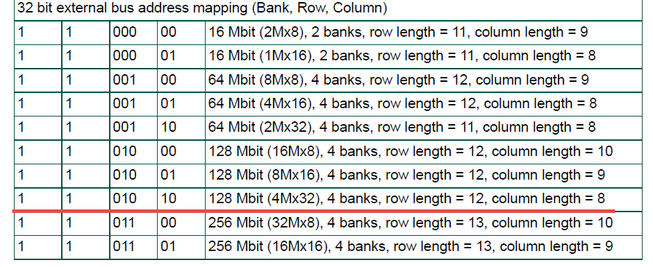
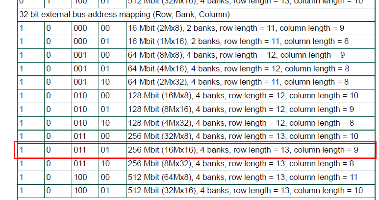
1) The table 134 of the attached file shows the possible configuration, can you tell me what I have to choose?
-- Please check the Fig 1.
Fig 1
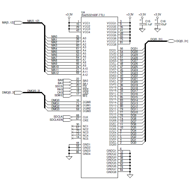
2) From the hardware point of view, is there any modifications to do?
-- No, just like you connect a 32-bit SDRAM(as the Fig2 shows).
Fig 2
Hope this is clear.
Have a great day,
TIC
-----------------------------------------------------------------------------------------------------------------------
Note: If this post answers your question, please click the Correct Answer button. Thank you!
-----------------------------------------------------------------------------------------------------------------------
- Mark as New
- Bookmark
- Subscribe
- Mute
- Subscribe to RSS Feed
- Permalink
- Report Inappropriate Content
Hi jeremyzhou,
I followed your indication but the new 512 Mbit memory doesn't work fine. Is there any setting I have to do?
The memory work fine (it seems to me) only if the address mapping bits 14:7 are as follow
bit 14=1
bit 13=0
bit 12=1
bit 11=0
bit 10=1
bit 9=0
bit 8=1
bit 7=0
but in this case the memory works as a 128 Mbit (4Mx32)
Have you any suggestion?
Many thanks.
- Mark as New
- Bookmark
- Subscribe
- Mute
- Subscribe to RSS Feed
- Permalink
- Report Inappropriate Content
Hi Nico Aprile,
Thank you for your reply.
Whether you tell me What the new 512Mb SDRAM you use.
Have a great day,
TIC
-----------------------------------------------------------------------------------------------------------------------
Note: If this post answers your question, please click the Correct Answer button. Thank you!
-----------------------------------------------------------------------------------------------------------------------
- Mark as New
- Bookmark
- Subscribe
- Mute
- Subscribe to RSS Feed
- Permalink
- Report Inappropriate Content
Hi, jeremyzhou,
old SDRAM (128 Mb) is the IS42S32400F model (http://www.issi.com/WW/pdf/42-45S32400F.pdf)
new SDRAM (512 Mb) is the IS42R32160F model (http://www.issi.com/WW/pdf/42-45R-S-32160F.pdf)
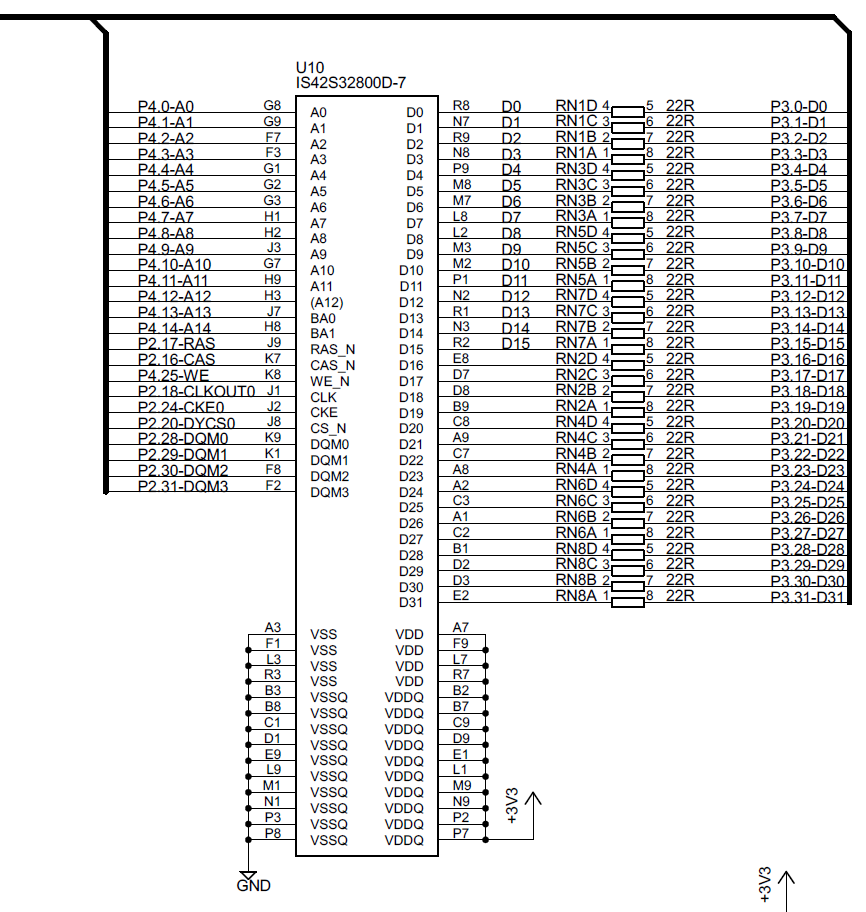
Below the new SDRAM connections
Attached you can find my SDRAM configuration and test code
Many thanks
Regards
- Mark as New
- Bookmark
- Subscribe
- Mute
- Subscribe to RSS Feed
- Permalink
- Report Inappropriate Content
Thanks for your reply.
1. It seems a bit weird that the SDRAM would work well after setting the addressing map as the Fig1 illustrates, it is definitely inconsistent with its datasheet. So I have no idea now.
Fig 1
2. I've attached an SDRAM demo, please use it as the template demo code and run it for testing.
Have a great day,
TIC
-------------------------------------------------------------------------------
Note:
- If this post answers your question, please click the "Mark Correct" button. Thank you!
- We are following threads for 7 weeks after the last post, later replies are ignored
Please open a new thread and refer to the closed one, if you have a
- Mark as New
- Bookmark
- Subscribe
- Mute
- Subscribe to RSS Feed
- Permalink
- Report Inappropriate Content
Hi jeremyzhou,
Now the SDRAM seems to work fine. I used the routines you sent me but I had to change something. I had to force the "add_mapped_p1" value. The routine modified is the following:
EMC_FUNC_CODE EMC_DynMemConfigAM(uint32_t index,
uint8_t addr_bus_width,
uint8_t addr_map,
uint8_t data_bus_width,
uint16_t chip_size)
{
const int chip_max_size = 512; // 512Mb
uint8_t data_bus_max_size = 0;
uint32_t add_mapped_p1 = 0x00, add_mapped_p2 = 0x00, add_mapped_p3 = 0x00;
uint32_t tmp = 16, i = 0, j = 0;
/* Get part 3 of address map */
switch(addr_bus_width)
{
case 16:
add_mapped_p3 = 0;
data_bus_max_size = 16;
break;
case 32:
add_mapped_p3 = 1;
data_bus_max_size = 32;
break;
default:
return EMC_FUNC_INVALID_PARAM;
}
/* Get part 2 of address map */
add_mapped_p2 = EMC_DYNAMIC_CFG_ADD_MAP_P2(addr_map);
/* Get part 1 of address map */
if(chip_size == 16)
{
if (data_bus_width == 8) add_mapped_p1 = 0;
else if(data_bus_width == 16) add_mapped_p1 = 1;
else return EMC_FUNC_INVALID_PARAM;
}
else
{
while(1)
{
i++;
tmp = 16*(0x01 << (i+1));
if(tmp == chip_size)
{
for(j = 0; (8<<j)<=data_bus_max_size;j++)
{
if((8<<j) == data_bus_width) break;
}
if( (8<<j) > data_bus_max_size) return EMC_FUNC_INVALID_PARAM;
add_mapped_p1 = (i<<2) + j;
break;
}
if(tmp >= chip_max_size)
{
return EMC_FUNC_INVALID_PARAM;
}
}
}
//SDRAM ISSI da 512 Mbit model IS42S32160F_7TLI 16Mx32 (4M x 32 bit x 4 bank)
add_mapped_p1=13; //
switch(index)
{
case 0:
LPC_EMC->DynamicConfig0 &= ~EMC_DYNAMIC_CFG_ADD_MAP_P1_MASK;
LPC_EMC->DynamicConfig0 |= EMC_DYNAMIC_CFG_ADD_MAP_P1(add_mapped_p1);
LPC_EMC->DynamicConfig0 &= ~EMC_DYNAMIC_CFG_ADD_MAP_P2_MASK;
LPC_EMC->DynamicConfig0 |= EMC_DYNAMIC_CFG_ADD_MAP_P2(add_mapped_p2);
LPC_EMC->DynamicConfig0 &= ~EMC_DYNAMIC_CFG_ADD_MAP_P3_MASK;
LPC_EMC->DynamicConfig0 |= EMC_DYNAMIC_CFG_ADD_MAP_P3(add_mapped_p3);
break;
case 1:
LPC_EMC->DynamicConfig1 &= ~EMC_DYNAMIC_CFG_ADD_MAP_P1_MASK;
LPC_EMC->DynamicConfig1 |= EMC_DYNAMIC_CFG_ADD_MAP_P1(add_mapped_p1);
LPC_EMC->DynamicConfig1 &= ~EMC_DYNAMIC_CFG_ADD_MAP_P2_MASK;
LPC_EMC->DynamicConfig1 |= EMC_DYNAMIC_CFG_ADD_MAP_P2(add_mapped_p2);
LPC_EMC->DynamicConfig1 &= ~EMC_DYNAMIC_CFG_ADD_MAP_P3_MASK;
LPC_EMC->DynamicConfig1 |= EMC_DYNAMIC_CFG_ADD_MAP_P3(add_mapped_p3);
break;
case 2:
LPC_EMC->DynamicConfig2 &= ~EMC_DYNAMIC_CFG_ADD_MAP_P1_MASK;
LPC_EMC->DynamicConfig2 |= EMC_DYNAMIC_CFG_ADD_MAP_P1(add_mapped_p1);
LPC_EMC->DynamicConfig2 &= ~EMC_DYNAMIC_CFG_ADD_MAP_P2_MASK;
LPC_EMC->DynamicConfig2 |= EMC_DYNAMIC_CFG_ADD_MAP_P2( add_mapped_p2);
LPC_EMC->DynamicConfig2 &= ~EMC_DYNAMIC_CFG_ADD_MAP_P3_MASK;
LPC_EMC->DynamicConfig2 |= EMC_DYNAMIC_CFG_ADD_MAP_P3(add_mapped_p3);
break;
case 3:
LPC_EMC->DynamicConfig3 &= ~EMC_DYNAMIC_CFG_ADD_MAP_P1_MASK;
LPC_EMC->DynamicConfig3 |= EMC_DYNAMIC_CFG_ADD_MAP_P1(add_mapped_p1);
LPC_EMC->DynamicConfig3 &= ~EMC_DYNAMIC_CFG_ADD_MAP_P2_MASK;
LPC_EMC->DynamicConfig3 |= EMC_DYNAMIC_CFG_ADD_MAP_P2(add_mapped_p2);
LPC_EMC->DynamicConfig3 &= ~EMC_DYNAMIC_CFG_ADD_MAP_P3_MASK;
LPC_EMC->DynamicConfig3 |= EMC_DYNAMIC_CFG_ADD_MAP_P3(add_mapped_p3);
break;
default:
return EMC_FUNC_INVALID_PARAM;
}
return EMC_FUNC_OK;
}The original routine calculated:
add_mapped_p1=17
add_mapped_p2=0
add_mapped_p3=1
but using add_mapped_p1=17 the SDRAM doesn't work fine. I have to force
add_mapped_p1=13
In this way the SDRAM works fine. Why your routine doesn't calcule the right add_mapped_p1 value?
The SDRAM timing I used are the following:
//SDRAM ISSI da 512 Mbit model IS42S32160F_7TLI 16Mx32 (4M x 32 bit x 4 bank)
config.ChipSize = 512; // 512 Mbit total
config.AddrBusWidth = 32; // 32 bit address bus
config.AddrMap = EMC_ADD_MAP_ROW_BANK_COL;
config.CSn = 0;
config.DataWidth = 16;
config.TotalSize = 536870912;
config.CASLatency = 2; // CAS
config.RASLatency = 1; // RAS
config.Active2ActivePeriod = 10; // tRC
config.ActiveBankLatency = 2; // tRRD
config.AutoRefrehPeriod = 10; // tRFC/tRC
config.DataIn2ActiveTime = 5; // tDAL, or tAPW
config.DataOut2ActiveTime = 5; // tAPR
config.WriteRecoveryTime = 2; // tWR, tDPL, tRWL, or tRDL
config.ExitSelfRefreshTime = EMC_NS2CLK(70); // tXSR
config.LoadModeReg2Active = 2; // tMRD
config.PrechargeCmdPeriod = 3; // tRP
config.ReadConfig = 1;
config.RefreshTime = EMC_SDRAM_REFRESH(64);
config.Active2PreChargeTime = 7; // tRAS
config.SeftRefreshExitTime = EMC_NS2CLK(70);
The configuration
add_mapped_p1=13
add_mapped_p2=0
add_mapped_p3=1
correspond to
Your previous suggestion was
I am a little bit confuse.. ![]() . Can you explain me?
. Can you explain me?
Many thanks
Regards
- Mark as New
- Bookmark
- Subscribe
- Mute
- Subscribe to RSS Feed
- Permalink
- Report Inappropriate Content
Hi Nico Aprile,
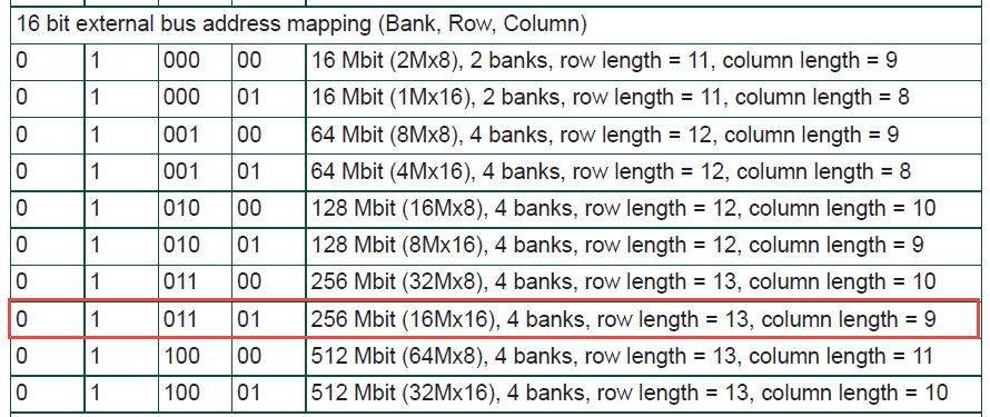
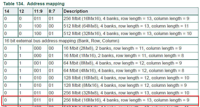
According to the below statement (Fig 1), the Fig 2 is correct, so I made a mistake before.
Hope this is clear.
Fig 1
Fig 2
Have a great day,
TIC
-------------------------------------------------------------------------------
Note:
- If this post answers your question, please click the "Mark Correct" button. Thank you!
- We are following threads for 7 weeks after the last post, later replies are ignored
Please open a new thread and refer to the closed one, if you have a related question at a later point in time.
-------------------------------------------------------------------------------
- Mark as New
- Bookmark
- Subscribe
- Mute
- Subscribe to RSS Feed
- Permalink
- Report Inappropriate Content
Hi jeremyzhou,
many, many thanks!
Your indication is:
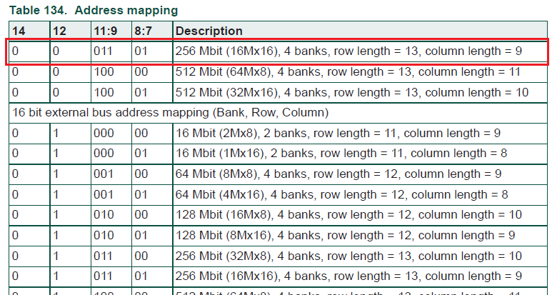
Why not the following?:
In other words, what's the bit 12 function
Have a nice day.
Regards
- Mark as New
- Bookmark
- Subscribe
- Mute
- Subscribe to RSS Feed
- Permalink
- Report Inappropriate Content
Hi Nico Aprile,
Thanks for your reply.
Actually, both are available.
However, It's the 16-bit external bus high-performance address mapping when the bit 12 is 0.
Have a great day,
TIC
-----------------------------------------------------------------------------------------------------------------------
Note: If this post answers your question, please click the Correct Answer button. Thank you!
-----------------------------------------------------------------------------------------------------------------------
- Mark as New
- Bookmark
- Subscribe
- Mute
- Subscribe to RSS Feed
- Permalink
- Report Inappropriate Content
jeremyzhou, I thank you very much!
Regards.


