- Forums
- Product Forums
- General Purpose MicrocontrollersGeneral Purpose Microcontrollers
- i.MX Forumsi.MX Forums
- QorIQ Processing PlatformsQorIQ Processing Platforms
- Identification and SecurityIdentification and Security
- Power ManagementPower Management
- Wireless ConnectivityWireless Connectivity
- RFID / NFCRFID / NFC
- Advanced AnalogAdvanced Analog
- MCX Microcontrollers
- S32G
- S32K
- S32V
- MPC5xxx
- Other NXP Products
- S12 / MagniV Microcontrollers
- Powertrain and Electrification Analog Drivers
- Sensors
- Vybrid Processors
- Digital Signal Controllers
- 8-bit Microcontrollers
- ColdFire/68K Microcontrollers and Processors
- PowerQUICC Processors
- OSBDM and TBDML
- S32M
- S32Z/E
-
- Solution Forums
- Software Forums
- MCUXpresso Software and ToolsMCUXpresso Software and Tools
- CodeWarriorCodeWarrior
- MQX Software SolutionsMQX Software Solutions
- Model-Based Design Toolbox (MBDT)Model-Based Design Toolbox (MBDT)
- FreeMASTER
- eIQ Machine Learning Software
- Embedded Software and Tools Clinic
- S32 SDK
- S32 Design Studio
- GUI Guider
- Zephyr Project
- Voice Technology
- Application Software Packs
- Secure Provisioning SDK (SPSDK)
- Processor Expert Software
- Generative AI & LLMs
-
- Topics
- Mobile Robotics - Drones and RoversMobile Robotics - Drones and Rovers
- NXP Training ContentNXP Training Content
- University ProgramsUniversity Programs
- Rapid IoT
- NXP Designs
- SafeAssure-Community
- OSS Security & Maintenance
- Using Our Community
-
- Cloud Lab Forums
-
- Knowledge Bases
- ARM Microcontrollers
- i.MX Processors
- Identification and Security
- Model-Based Design Toolbox (MBDT)
- QorIQ Processing Platforms
- S32 Automotive Processing Platform
- Wireless Connectivity
- CodeWarrior
- MCUXpresso Suite of Software and Tools
- MQX Software Solutions
- RFID / NFC
- Advanced Analog
-
- NXP Tech Blogs
- Home
- :
- General Purpose Microcontrollers
- :
- LPC Microcontrollers
- :
- Re: LPC1778 CS/OE_Enable interval length?
LPC1778 CS/OE_Enable interval length?
- Subscribe to RSS Feed
- Mark Topic as New
- Mark Topic as Read
- Float this Topic for Current User
- Bookmark
- Subscribe
- Mute
- Printer Friendly Page
LPC1778 CS/OE_Enable interval length?
- Mark as New
- Bookmark
- Subscribe
- Mute
- Subscribe to RSS Feed
- Permalink
- Report Inappropriate Content
Hello,
When using LPC1778 with 32-bit External Memory interface,
(refer to cmsis-RTOS)
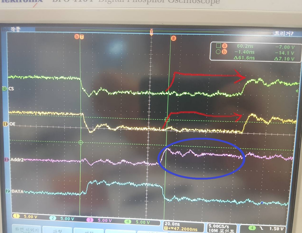
CS / OE selection interval is set to 60ns, but the actual operation is doubled with 100ns.
CS & OE ENABLE Interval timing is 2times longer than Address & Data.
How to reduce these CS & OE ENABLE interval timing such as Address/Data interval length?
(CS : Green, OE : Yellow, Addr : violet, DATA : Blue)
in order to operate same interval length exactly between CS/OE and Address/Data.
It's occurred address changing(0 ->1 : Blue circle) due to 2-times longer interval length.
How to change such as RED line in drawing signal waveform attached?
1. Issues :
1) CS3 setting value is set to operate at about 60ns as shown below, but 100ns actually appears
2) ADDR changes while maintaining CS3 LOW (CS is changed once after 60ns in 120ns interval)
3) When CS3 is output as 120ns, it is outputted as 60ns every 16th.
2. Reference :
CS related setting value
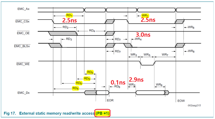
* PB = 1
Set. value | Tcy(clk) | 60MHz |
16.7ns | ||
WAITEN | 0 | |
WAITWR | 5 | |
WAITOEN | 0 | |
WAITRD | 2 | |
WAITPAGE | 2 | |
WAITRETURN | 1 | |
Cal. vaule | RD2 | 2.5ns |
RD4 | 48.4ns | |
RD5 | 34.5ns |
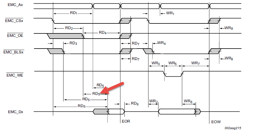
3. look at the Timing diagram as below, there are four RD5s,
Which is the standard? or What is the standard?
Best regards,
eric
- Mark as New
- Bookmark
- Subscribe
- Mute
- Subscribe to RSS Feed
- Permalink
- Report Inappropriate Content
Hi Jeremyzhou,
What do I need to do verify it?
Could you have any additional updates?
for example, sample code that can be verified or reference design, so on.
Best regards,
eric
- Mark as New
- Bookmark
- Subscribe
- Mute
- Subscribe to RSS Feed
- Permalink
- Report Inappropriate Content
Hi eric kim,
Thank you for your interest in NXP Semiconductor products and for the opportunity to serve you.
1. The Interval timing between CS and OE_ENABLE is RD2, do you mean that this timing value becomes the 100 ns, not the 60ns as the expected? If yes, I don't find this issue exists in the figure.
So I was wondering if you can attach the figure which contains more wave, it can illustrate the issue more clearly.
2. From the top to below, The second RD5 is standard.
Have a great day,
TIC
-----------------------------------------------------------------------------------------------------------------------
Note: If this post answers your question, please click the Correct Answer button. Thank you!
-----------------------------------------------------------------------------------------------------------------------
- Mark as New
- Bookmark
- Subscribe
- Mute
- Subscribe to RSS Feed
- Permalink
- Report Inappropriate Content
Hi Jeremyzhou,
Thank you for the reply,
1. I mean that CS (or OE) Low active selection interval length is set to 60ns, but the CS or OE actual Low active length is 100ns, that means double length against I want to set 60ns.
You can see the above attached waveform's Delta 61.6ns timing vertical Line from (a) to (b).
Best regards,
eric
- Mark as New
- Bookmark
- Subscribe
- Mute
- Subscribe to RSS Feed
- Permalink
- Report Inappropriate Content
Hi eric kim,
Thanks for your reply.
I'd like to get the more information and whether you can clarify the below inquiries.
1. The above figure shows a read operation, I was wondering if you can share the complete wave and the corresponding code.
2. Whether you can share the SCH of the static flash.
Have a great day,
TIC
-----------------------------------------------------------------------------------------------------------------------
Note: If this post answers your question, please click the Correct Answer button. Thank you!
-----------------------------------------------------------------------------------------------------------------------
- Mark as New
- Bookmark
- Subscribe
- Mute
- Subscribe to RSS Feed
- Permalink
- Report Inappropriate Content
- Mark as New
- Bookmark
- Subscribe
- Mute
- Subscribe to RSS Feed
- Permalink
- Report Inappropriate Content
Hi eric kim,
It becomes a bit complicated. I was if you can clarify these questions.
1) Does the LPC1788 connect the FPGA: XC6SLX4-2CSG225C?
2) Actually, the code doesn't provide enough information for me to figure the operation as the above figure shows.
So please upload a compile-able demo.
3) I suspect the instable address is the root cause, to confirm it, I'd highly recommend you to use the logic analyzer to visualize the CS, OE, ADDR and DATA pins
Have a great day,
TIC
-----------------------------------------------------------------------------------------------------------------------
Note: If this post answers your question, please click the Correct Answer button. Thank you!
-----------------------------------------------------------------------------------------------------------------------
- Mark as New
- Bookmark
- Subscribe
- Mute
- Subscribe to RSS Feed
- Permalink
- Report Inappropriate Content
Hi, Jeremyzhou,
pls refer to the attached EMC code setting, CPU setting and a waveform.
I have question about LPC1778 READ Timming.
Setup time is under review to reduce read time.
In FPGA READ, access to CS twice by 16bits at a time.
OE operates in the same way as CS and it is difficult to know the sampling timing.
If OE operation is correct? and If correct, How to know CPU sampling timing?
In addition, ADDR is not maintained until the end of CS/OE,
Is this the right behavior?
If you have 16bit read timing chart, please let me know.
Thank you,
eric
- Mark as New
- Bookmark
- Subscribe
- Mute
- Subscribe to RSS Feed
- Permalink
- Report Inappropriate Content
Hi eric kim,
In your original question, you said 'CS / OE selection interval is set to 60ns, but the actual operation is doubled with 100ns', Fig 17 illustrates one read cycle and one write cycle.
However, in the continual read process, the CS and OE will keep low, so this phenomenon is normal.
After reviewing the attachment, I find that MW=1(16 bit), but you actual use the 32 bit as SCH shows.
Note:
If a memory bank is configured to be 32 bits wide, address lines A0 and A1 can be used
as non-address lines. If a memory bank is configured to 16 bits wide, A0 is not required.
However, 8 bit wide memory banks do require all address lines down to A0. Configuring
the A1 and/or A0 lines to provide address or non-address function is accomplished using
the IOCON registers.
Another problem is PB bit should be asserted 0.
Regarding to your implementation, I'd highly recommend you to refer to a parallel-Nor flash's datasheet if you want to use the FPGA to simulate it, for instance, SST38VF6401.
Have a great day,
TIC
-----------------------------------------------------------------------------------------------------------------------
Note: If this post answers your question, please click the Correct Answer button. Thank you!
-----------------------------------------------------------------------------------------------------------------------


