- Forums
- Product Forums
- General Purpose MicrocontrollersGeneral Purpose Microcontrollers
- i.MX Forumsi.MX Forums
- QorIQ Processing PlatformsQorIQ Processing Platforms
- Identification and SecurityIdentification and Security
- Power ManagementPower Management
- Wireless ConnectivityWireless Connectivity
- RFID / NFCRFID / NFC
- Advanced AnalogAdvanced Analog
- MCX Microcontrollers
- S32G
- S32K
- S32V
- MPC5xxx
- Other NXP Products
- S12 / MagniV Microcontrollers
- Powertrain and Electrification Analog Drivers
- Sensors
- Vybrid Processors
- Digital Signal Controllers
- 8-bit Microcontrollers
- ColdFire/68K Microcontrollers and Processors
- PowerQUICC Processors
- OSBDM and TBDML
- S32M
- S32Z/E
-
- Solution Forums
- Software Forums
- MCUXpresso Software and ToolsMCUXpresso Software and Tools
- CodeWarriorCodeWarrior
- MQX Software SolutionsMQX Software Solutions
- Model-Based Design Toolbox (MBDT)Model-Based Design Toolbox (MBDT)
- FreeMASTER
- eIQ Machine Learning Software
- Embedded Software and Tools Clinic
- S32 SDK
- S32 Design Studio
- GUI Guider
- Zephyr Project
- Voice Technology
- Application Software Packs
- Secure Provisioning SDK (SPSDK)
- Processor Expert Software
- Generative AI & LLMs
-
- Topics
- Mobile Robotics - Drones and RoversMobile Robotics - Drones and Rovers
- NXP Training ContentNXP Training Content
- University ProgramsUniversity Programs
- Rapid IoT
- NXP Designs
- SafeAssure-Community
- OSS Security & Maintenance
- Using Our Community
-
- Cloud Lab Forums
-
- Knowledge Bases
- ARM Microcontrollers
- i.MX Processors
- Identification and Security
- Model-Based Design Toolbox (MBDT)
- QorIQ Processing Platforms
- S32 Automotive Processing Platform
- Wireless Connectivity
- CodeWarrior
- MCUXpresso Suite of Software and Tools
- MQX Software Solutions
- RFID / NFC
- Advanced Analog
-
- NXP Tech Blogs
- Home
- :
- General Purpose Microcontrollers
- :
- LPC Microcontrollers
- :
- Custom Pin Configuration Using LPC55S69-EVK
Custom Pin Configuration Using LPC55S69-EVK
- Subscribe to RSS Feed
- Mark Topic as New
- Mark Topic as Read
- Float this Topic for Current User
- Bookmark
- Subscribe
- Mute
- Printer Friendly Page
Custom Pin Configuration Using LPC55S69-EVK
- Mark as New
- Bookmark
- Subscribe
- Mute
- Subscribe to RSS Feed
- Permalink
- Report Inappropriate Content
I'm working with a LPC55S69-EVK to integrate a number of custom sensors utilizing various communication protocols. I'll be writing custom software that references the generated code from Pins and Peripherals. In other words, I won't be using LPC examples or their configurations.
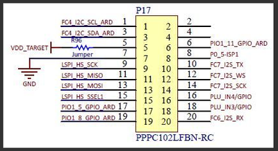
Looking at the LPC55S69-EVK Board Schematic, the pinouts from P16-P19 look promising. However, I'm struggling to identify the actual routing of each pin on the board. It's possible for me to go through and run a continuity check on every pin and map it out myself, but also thought that a document or something similar has to exist that shows the pin-level routing for custom applications.
For example, P17 pin 1 is mapped to FC4_I2C_SCL_ARD. Referencing the images below, does that map to pin 88 or pin 30 in the MCUXpresso Pins Tool? I have a similar question for a lot of the pins that are shown in the schematic and having some kind of document to reference would drastically reduce the work of checking continuity of every LPC pin.
- Mark as New
- Bookmark
- Subscribe
- Mute
- Subscribe to RSS Feed
- Permalink
- Report Inappropriate Content
Hi,
For the LPC55S69-EVK pin name, as you know that the Port pin is unique and map to only one pin. For example, for the pin 1 of P17, it is FC4_I2C_SCL_ARD, you can search on the schematics with pdf format,
By searching the key word "FC4_I2C_SCL_ARD", you can see that the the node corresponds PIO1_20 or pin 4 of LPC5569.
You can configure the PIO1_20 as FC4_I2C_SCLK, it is okay.
From hardware register configuration, each GPIO pin corresponds to a IOCON register, you can set up the FUNC bit to determine the pin function.
There is not doc which describes the map between the signal name and pin map for the EVK board.
Hope it can help you
BR
XiangJun Rong


