
- Forums
- Product Forums
- General Purpose MicrocontrollersGeneral Purpose Microcontrollers
- i.MX Forumsi.MX Forums
- QorIQ Processing PlatformsQorIQ Processing Platforms
- Identification and SecurityIdentification and Security
- Power ManagementPower Management
- Wireless ConnectivityWireless Connectivity
- RFID / NFCRFID / NFC
- Advanced AnalogAdvanced Analog
- Neural Processing UnitsNeural Processing Units
- MCX Microcontrollers
- S32G
- S32K
- S32V
- MPC5xxx
- Other NXP Products
- S12 / MagniV Microcontrollers
- Powertrain and Electrification Analog Drivers
- Sensors
- Vybrid Processors
- Digital Signal Controllers
- 8-bit Microcontrollers
- ColdFire/68K Microcontrollers and Processors
- PowerQUICC Processors
- OSBDM and TBDML
- S32M
- S32Z/E
-
- Solution Forums
- Software Forums
- MCUXpresso Software and ToolsMCUXpresso Software and Tools
- CodeWarriorCodeWarrior
- MQX Software SolutionsMQX Software Solutions
- Model-Based Design Toolbox (MBDT)Model-Based Design Toolbox (MBDT)
- FreeMASTER
- eIQ Machine Learning Software
- Embedded Software and Tools Clinic
- S32 SDK
- S32 Design Studio
- GUI Guider
- Zephyr Project
- Voice Technology
- Application Software Packs
- Secure Provisioning SDK (SPSDK)
- Processor Expert Software
- Generative AI & LLMs
-
- Topics
- Mobile Robotics - Drones and RoversMobile Robotics - Drones and Rovers
- NXP Training ContentNXP Training Content
- University ProgramsUniversity Programs
- Rapid IoT
- NXP Designs
- SafeAssure-Community
- OSS Security & Maintenance
- Using Our Community
-
- Cloud Lab Forums
-
- Knowledge Bases
- ARM Microcontrollers
- i.MX Processors
- Identification and Security
- Model-Based Design Toolbox (MBDT)
- QorIQ Processing Platforms
- S32 Automotive Processing Platform
- Wireless Connectivity
- CodeWarrior
- MCUXpresso Suite of Software and Tools
- MQX Software Solutions
- RFID / NFC
- Advanced Analog
- Neural Processing Units
-
- NXP Tech Blogs
- Home
- :
- 汎用マイクロコントローラ
- :
- LPCマイクロコントローラ
- :
- Re: Controlling WS2812 LED Strips with the LPC810
Controlling WS2812 LED Strips with the LPC810
オプション
- RSS フィードを購読する
- トピックを新着としてマーク
- トピックを既読としてマーク
- このトピックを現在のユーザーにフロートします
- ブックマーク
- 購読
- ミュート
- 印刷用ページ
Controlling WS2812 LED Strips with the LPC810
06-15-2016
01:03 PM
39,535件の閲覧回数
NXP Employee
- 新着としてマーク
- ブックマーク
- 購読
- ミュート
- RSS フィードを購読する
- ハイライト
- 印刷
- 不適切なコンテンツを報告
Content originally posted in LPCWare by cpldcpu on Mon Jul 29 11:25:41 MST 2013
I ported my light weight WS2812 to the LPC810. The WS2812 is an RGB LED with an integrated controller that uses a 800kHz serial NRZ protocol to transmit 24 bit RGB data. Due to the nature of the protocol, it is quite incompatible to what most SPI units support.
I implemented a bitbanging approach with active CPU waiting. This requires predictable code execution timing. Luckily the LPC810 supports zero waitstate code memory access up to 30 Mhz. One advantage of the LPC810 is the relatively large SRAM compared to the code memory. 1024 bytes of sram allow controlling a full strip. A full 4m strip contains 240 LEDS and requires 3*240=720 bytes of memory. Most of the small 8 bit controllers only have 512 bytes or less.
You can see my code in action here: http://www.youtube.com/watch?v=Uwxt7SuSV7Y
Current state of the library: https://github.com/cpldcpu/light_ws2812/tree/master/light_ws2812_ARM
I have been considering to use the SCT to get rid of the reliance on code exection timing. Unfortunately it seems that this will still not free up CPU timing, as the interrupt overhead would not allow 800kHz clocking. Maybe it is possible to use internal pin forwarding to combine SPI and SCT to implement this protocol?
22 返答(返信)
06-15-2016
01:04 PM
37,188件の閲覧回数
NXP Employee
- 新着としてマーク
- ブックマーク
- 購読
- ミュート
- RSS フィードを購読する
- ハイライト
- 印刷
- 不適切なコンテンツを報告
Content originally posted in LPCWare by riscy00 on Thu May 07 22:50:50 MST 2015
Hi
I pickup your code and make it work under LPCOpen style on actual LPC812 device. Using LPC812-MAX EVAL board. It working very nicely.
The P0.16 and P0.17 connect to LED port which is not optimal. I wish to move it P0.14 and P0.15 but no longer work. I checked datasheet and SCT and could find out why. I'm open for suggestion or reason to explain this. Below is the sample code, the top is for Pin 17/18 (WB2812B_GPIO_Setup) which worked and bottom is Pin 15/16 (WB2812B_GPIO_Setup_1415)
//==================================================================
//================================================================== WB2812B_GPIO_Setup
// Purpose: Setup GPIO for this project.
// Input:
// Output:
// Note : Pin 7 shared with heartbeat for activity indicator, but green is too strong to see red.
//: Pin 4 CTOUT_0 connect to LED string with DIN pin
//: Pin 16 SCK0 connect to CTIN_0 internally.
//: Pin 17 MOSI0 connect to CTIN_1 internally.
//==================================================================
void WB2812B_GPIO_Setup(void)
{
Chip_Clock_EnablePeriphClock(SYSCTL_CLOCK_SPI0);//enable SPI0 clock
Chip_Clock_EnablePeriphClock(SYSCTL_CLOCK_SCT);//enable SCT clock
//--------------------------------------------Activate the SWM
Chip_Clock_EnablePeriphClock(SYSCTL_CLOCK_SWM);
//--------------------------------------------LED Indicator
Chip_GPIO_SetPinDIROutput(LPC_GPIO_PORT, 0, 7);
//--------------------------------------------Routing SPI over P0.16/P.17 which are not external pins on LPC810
Chip_SWM_MovablePinAssign(SWM_SPI0_SCK_IO, 16);//P0.16 = SCK0
Chip_SWM_MovablePinAssign(SWM_SPI0_MOSI_IO,17);//P0.17 = MOSI0
//--------------------------------------------Rounting CTIN0,CTIN1 and CTOUT
Chip_SWM_MovablePinAssign(SWM_CTIN_0_I,16);//P0.16 = CTIN_0 connect to SCK0
Chip_SWM_MovablePinAssign(SWM_CTIN_1_I,17);//P0.17 = CTIN_1 connect to MOSI0
Chip_SWM_MovablePinAssign(SWM_CTOUT_0_O,4);//P0.04 = CTOUT_0  WS2812B data out to LED string.
//--------------------------------------------Deactivate the SWM to save power.
Chip_Clock_DisablePeriphClock(SYSCTL_CLOCK_SWM);
}

void WB2812B_GPIO_Setup_1415(void)
{
Chip_Clock_EnablePeriphClock(SYSCTL_CLOCK_SPI0);//enable SPI0 clock
Chip_Clock_EnablePeriphClock(SYSCTL_CLOCK_SCT);//enable SCT clock
//--------------------------------------------Activate the SWM
Chip_Clock_EnablePeriphClock(SYSCTL_CLOCK_SWM);
//--------------------------------------------LED Indicator
Chip_GPIO_SetPinDIROutput(LPC_GPIO_PORT, 0, 7);
//--------------------------------------------Routing SPI over P0.16/P.17 which are not external pins on LPC810
Chip_SWM_MovablePinAssign(SWM_SPI0_SCK_IO, 14);//P0.14 = SCK0
Chip_SWM_MovablePinAssign(SWM_SPI0_MOSI_IO,15);//P0.15 = MOSI0
//--------------------------------------------Rounting CTIN0,CTIN1 and CTOUT
Chip_SWM_MovablePinAssign(SWM_CTIN_0_I,14);//P0.14 = CTIN_0 connect to SCK0
Chip_SWM_MovablePinAssign(SWM_CTIN_1_I,15);//P0.15 = CTIN_1 connect to MOSI0
Chip_SWM_MovablePinAssign(SWM_CTOUT_0_O,4);//P0.04 = CTOUT_0  WS2812B data out to LED string.
//--------------------------------------------Deactivate the SWM to save power.
Chip_Clock_DisablePeriphClock(SYSCTL_CLOCK_SWM);
}
|
06-15-2016
01:04 PM
37,188件の閲覧回数
NXP Employee
- 新着としてマーク
- ブックマーク
- 購読
- ミュート
- RSS フィードを購読する
- ハイライト
- 印刷
- 不適切なコンテンツを報告
Content originally posted in LPCWare by markr on Tue Sep 24 15:07:39 MST 2013
this posting sort of answers the question:
http://www.lpcware.com/content/forum/lpc810-question-about-connect-acmpo-sct-input#comment-1131496
From NPX_Paul:
Quote:
It is never a good idea to use a pin that does not exist in the device data sheet. Although it may work in some situations, there is no guarantee that it will continue to function correctly in future device revisions.
06-15-2016
01:04 PM
37,192件の閲覧回数
NXP Employee
- 新着としてマーク
- ブックマーク
- 購読
- ミュート
- RSS フィードを購読する
- ハイライト
- 印刷
- 不適切なコンテンツを報告
Content originally posted in LPCWare by rickta59 on Sat Aug 17 06:35:36 MST 2013
DIP 8 devices with rev. 2A
DIP 8 devices with rev. 2A
06-15-2016
01:04 PM
37,194件の閲覧回数
NXP Employee
- 新着としてマーク
- ブックマーク
- 購読
- ミュート
- RSS フィードを購読する
- ハイライト
- 印刷
- 不適切なコンテンツを報告
Content originally posted in LPCWare by cpldcpu on Sat Aug 17 05:49:03 MST 2013
Quote: fjrg76
Where did you buy the LPC800 chips? mouser.com and digi-key.com have no stock, so I cannot start any projects based in such a family, and the LPCXpresso board is not suitable for production purposes.
Any ideas?
I got mine as part of the mini-kit in NXPs giveaway. Apparently there are samples available at the official distributors, but they are not selling the device yet. It may be worth calling them...
Ricka: Which one is the version with the broken comparator? The price of Adafruits offering is a bit steep. The parts are hardly worth more than $5...
06-15-2016
01:04 PM
37,194件の閲覧回数
NXP Employee
- 新着としてマーク
- ブックマーク
- 購読
- ミュート
- RSS フィードを購読する
- ハイライト
- 印刷
- 不適切なコンテンツを報告
Content originally posted in LPCWare by rickta59 on Sat Aug 17 05:44:09 MST 2013
Adafruit sells the lpc810 chip and a usb dongle as a kit. I really only wanted the chip. Unfortunately, that is the only place I've seen with any stock. Also, the chip they sent me is the revision that has the faulty comparator.
Adafruit sells the lpc810 chip and a usb dongle as a kit. I really only wanted the chip. Unfortunately, that is the only place I've seen with any stock. Also, the chip they sent me is the revision that has the faulty comparator.
06-15-2016
01:04 PM
37,194件の閲覧回数
NXP Employee
- 新着としてマーク
- ブックマーク
- 購読
- ミュート
- RSS フィードを購読する
- ハイライト
- 印刷
- 不適切なコンテンツを報告
Content originally posted in LPCWare by fjrg76 on Thu Aug 15 13:06:30 MST 2013
Where did you buy the LPC800 chips? mouser.com and digi-key.com have no stock, so I cannot start any projects based in such a family, and the LPCXpresso board is not suitable for production purposes.
Any ideas?
Where did you buy the LPC800 chips? mouser.com and digi-key.com have no stock, so I cannot start any projects based in such a family, and the LPCXpresso board is not suitable for production purposes.
Any ideas?
06-15-2016
01:04 PM
37,194件の閲覧回数
NXP Employee
- 新着としてマーク
- ブックマーク
- 購読
- ミュート
- RSS フィードを購読する
- ハイライト
- 印刷
- 不適切なコンテンツを報告
Content originally posted in LPCWare by cpldcpu on Tue Aug 13 00:21:09 MST 2013
Quote: LPChobbyist
In general, my plan is to move all input-output functions (i.e. SCK/MOSI/SCT inputs) to the pins not bonded out on the physical (8-pin) package so that I could add more input/out functionality that actually needs interaction with the real world to the remaining few pins. I hope NXP keeps the existing switch matrix behavior in the future products because I like it a lot:-). One thing I hope also works is to connect multiple input functions to the same physical pin – i.e. I can configure one SCT input to track rising edges, another input to track falling edges and using both of them I can easily get pulse length.
Yes, that is a very elegant solution. It would helpful if NXP could comment on "feature". Connecting more than one input to a single pin is allowable per the user manual.
Quote: LPChobbyist
As for how much of other resources (Flash, SRAM) is available on a particular die, my rule of the thumb is to trust the DS/UM. Whenever I would talk to NXP people about if there is more of something on the chip or not, they would underline that even if one gets lucky with a particular revision of the device and gets some bonus feature(s) present, it can easily be revoked/fixed/removed/trimmed in the next design cycle so that it would match the official spec. So far I played it safe and did not get surprised.
Well, if you want your application to work, you should stick to the specification, that is obvious. Many MCU vendors use the same die across a range
of products and define the product only at test by fusing or different package options. I strongly suspect that the same is the case for the LPC800 series. However, even if additional memory is present in the LPC810, it may be disabled in a way that makes it impossible to reactivate without physically altering the device.
Quote: LPChobbyist
In general, my plan is to move all input-output functions (i.e. SCK/MOSI/SCT inputs) to the pins not bonded out on the physical (8-pin) package so that I could add more input/out functionality that actually needs interaction with the real world to the remaining few pins. I hope NXP keeps the existing switch matrix behavior in the future products because I like it a lot:-). One thing I hope also works is to connect multiple input functions to the same physical pin – i.e. I can configure one SCT input to track rising edges, another input to track falling edges and using both of them I can easily get pulse length.
Yes, that is a very elegant solution. It would helpful if NXP could comment on "feature". Connecting more than one input to a single pin is allowable per the user manual.
Quote: LPChobbyist
As for how much of other resources (Flash, SRAM) is available on a particular die, my rule of the thumb is to trust the DS/UM. Whenever I would talk to NXP people about if there is more of something on the chip or not, they would underline that even if one gets lucky with a particular revision of the device and gets some bonus feature(s) present, it can easily be revoked/fixed/removed/trimmed in the next design cycle so that it would match the official spec. So far I played it safe and did not get surprised.
Well, if you want your application to work, you should stick to the specification, that is obvious. Many MCU vendors use the same die across a range
of products and define the product only at test by fusing or different package options. I strongly suspect that the same is the case for the LPC800 series. However, even if additional memory is present in the LPC810, it may be disabled in a way that makes it impossible to reactivate without physically altering the device.
06-15-2016
01:03 PM
37,194件の閲覧回数
NXP Employee
- 新着としてマーク
- ブックマーク
- 購読
- ミュート
- RSS フィードを購読する
- ハイライト
- 印刷
- 不適切なコンテンツを報告
Content originally posted in LPCWare by LPChobbyist on Mon Aug 12 12:03:43 MST 2013
Hi cpldcpu,
Since I have the LPC812 board and the LPC800-Mini-kit and I used both of them when developing the SPI+SCT WS2812 demo. I observed the same behavior regarding the pins not available on the 8-pin package as you have described here, however for the sake of illustrating the SPI+SCT interaction I decided to use the pins on the 8-pin package I could probe.
In general, my plan is to move all input-output functions (i.e. SCK/MOSI/SCT inputs) to the pins not bonded out on the physical (8-pin) package so that I could add more input/out functionality that actually needs interaction with the real world to the remaining few pins. I hope NXP keeps the existing switch matrix behavior in the future products because I like it a lot:-). One thing I hope also works is to connect multiple input functions to the same physical pin – i.e. I can configure one SCT input to track rising edges, another input to track falling edges and using both of them I can easily get pulse length.
As for how much of other resources (Flash, SRAM) is available on a particular die, my rule of the thumb is to trust the DS/UM. Whenever I would talk to NXP people about if there is more of something on the chip or not, they would underline that even if one gets lucky with a particular revision of the device and gets some bonus feature(s) present, it can easily be revoked/fixed/removed/trimmed in the next design cycle so that it would match the official spec. So far I played it safe and did not get surprised.
06-15-2016
01:03 PM
37,194件の閲覧回数
NXP Employee
- 新着としてマーク
- ブックマーク
- 購読
- ミュート
- RSS フィードを購読する
- ハイライト
- 印刷
- 不適切なコンテンツを報告
Content originally posted in LPCWare by cpldcpu on Sun Aug 11 01:58:12 MST 2013
After consulting the manual a bit:
It is stated that the switch matrix is identical in all LPC800 devices. The GPIO output devices are apparently separate from the switch matrix and fixed per pin.
However, as shown in Figure 7 on page 16 of the datasheet, input and output of a pin are only connected after the output driver (which makes a lot of sense). So, that means that internal signals are also forwarded across GPIO drivers or is there an internal bypass? It would surprise me a bit if the LPC810 die had all the 18 GPIO output drivers as they are probably quite area intensive. But then again, the LPC810 is probably not the most optimized part of the family...
06-15-2016
01:03 PM
37,192件の閲覧回数
NXP Employee
- 新着としてマーク
- ブックマーク
- 購読
- ミュート
- RSS フィードを購読する
- ハイライト
- 印刷
- 不適切なコンテンツを報告
Content originally posted in LPCWare by cpldcpu on Sun Aug 11 00:18:24 MST 2013
Hi LPChobbyist,
I played a bit around with your code. You developed this on an LPC812 board, right? There is some interference with the RS232 connection on the LPC810 mini-kit when using your pin assignments, since P0.04 is used for both the WS2812 data output and the RX connection. I fixed this by moving the data output to P0.02 and removing the two indicator outputs to save pins.
When moving around the pins used for the SPI/SCT connection I found something very interesting: It is also possible to use pins other than P0.00 to P0.05, which are available on the LPC810. In fact up to P0.17 can be successfully used to forward signals internally. P0.18 fails. This makes a lot of sense, since P0.17 is the highest GPIO pin on the LPC812. This finding is very useful, since it allows connecting peripheral devices internally without wasting output pins on the small pin count devices.
Is this undocumented feature something that can be used reliably? Or may it go away in future silicon revisions? Are the GPIO output drivers actually present on the die and are not bonded, or is the forwarding done in an energy saving way within the switch matrix? Can one of the NXP guys answer this?
This also begs the question, whether the LPC810 die also has 16kb flash and 4kb ram. Is the entire LPC800 series using the same die? This needs further poking around...
Please find attached my updated version of LPChobbyists code for the LPC810.
06-15-2016
01:03 PM
37,192件の閲覧回数
NXP Employee
- 新着としてマーク
- ブックマーク
- 購読
- ミュート
- RSS フィードを購読する
- ハイライト
- 印刷
- 不適切なコンテンツを報告
Content originally posted in LPCWare by LPChobbyist on Fri Aug 09 16:37:20 MST 2013
Hi SCT guys,
Just realized I said “A falling edge on CTIN0...” in the description of the limiting event. This is not correct.
It is “A rising edge on CTIN0...”, as it was implemented in the demo (and mentioned in comments in main.c). For the selected SPI configuration (CPHA=1, CPOL=1) SCK’s rising edges are the sampling edges and this is when the MOSI data are guaranteed to be stable...
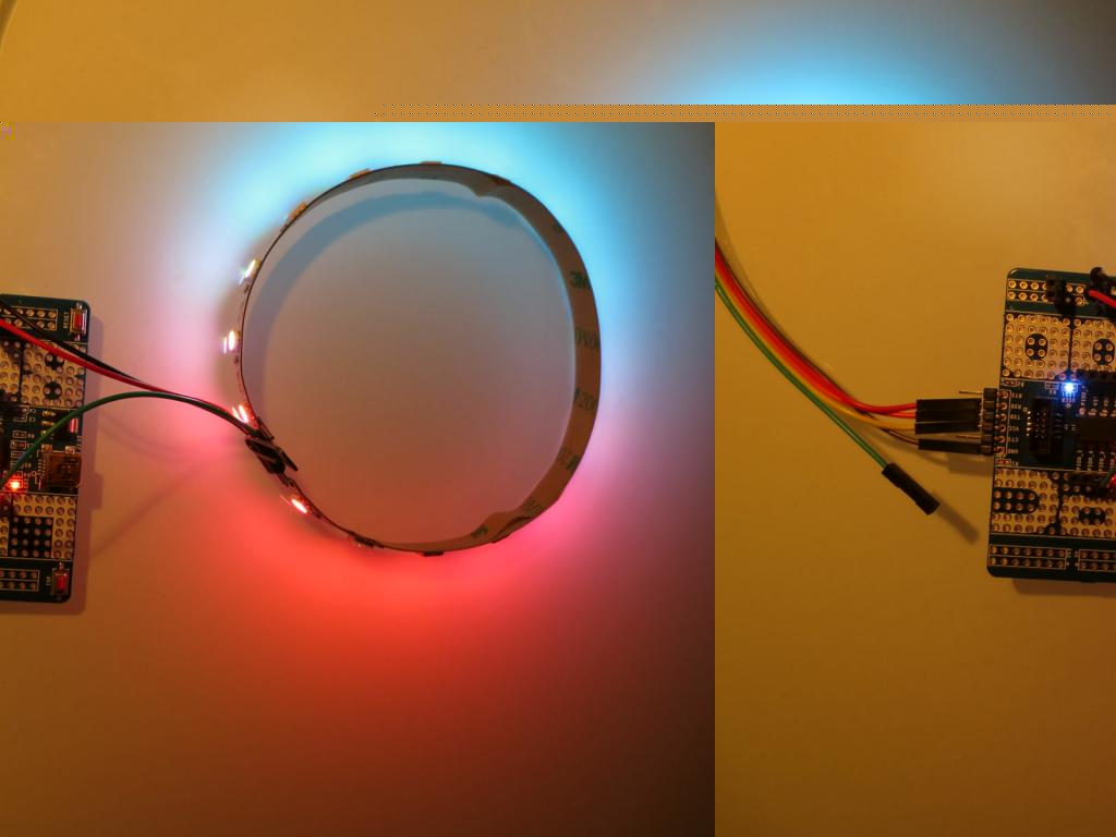
Here is a video showing my LPC810 SPI+SCT & WS2812 demo running. The rightmost LED is LED0, the central one is LED1 while the leftmost LED is LED2.
http://www.youtube.com/watch?v=uWiSp9bJei0
Hi SCT guys,
Just realized I said “A falling edge on CTIN0...” in the description of the limiting event. This is not correct.
It is “A rising edge on CTIN0...”, as it was implemented in the demo (and mentioned in comments in main.c). For the selected SPI configuration (CPHA=1, CPOL=1) SCK’s rising edges are the sampling edges and this is when the MOSI data are guaranteed to be stable...
Here is a video showing my LPC810 SPI+SCT & WS2812 demo running. The rightmost LED is LED0, the central one is LED1 while the leftmost LED is LED2.
http://www.youtube.com/watch?v=uWiSp9bJei0
06-15-2016
01:03 PM
37,192件の閲覧回数
NXP Employee
- 新着としてマーク
- ブックマーク
- 購読
- ミュート
- RSS フィードを購読する
- ハイライト
- 印刷
- 不適切なコンテンツを報告
Content originally posted in LPCWare by LPChobbyist on Fri Aug 09 15:50:55 MST 2013
Quote: cpldcpu
LPCHobbyist, great work! That is exactly what I hoped to implement. I like the idea of also forwarding SCK to the SCT. I planned to do this by software synchronization, but your approach is of course much more robust and also allows detection of the reset conditition.
I have to play a bit with the code to understand it more. The SCT is still a bit confusing to me.
Hello cpldcpu,
Thank you!
The SCT is a powerful peripheral on NXP’s micros and I used it on several projects. It takes a while to get used to it but once you become comfortable around it sky is the limit:-).
06-15-2016
01:03 PM
37,192件の閲覧回数
NXP Employee
- 新着としてマーク
- ブックマーク
- 購読
- ミュート
- RSS フィードを購読する
- ハイライト
- 印刷
- 不適切なコンテンツを報告
Content originally posted in LPCWare by LPChobbyist on Fri Aug 09 12:46:01 MST 2013
Hello Rick,
Thank you!
Yes, I did hand code the SCT registers in this case. I know of the Red State tool but have not used it so far. I will try it and will let you know how it goes.
Hello Rick,
Thank you!
Yes, I did hand code the SCT registers in this case. I know of the Red State tool but have not used it so far. I will try it and will let you know how it goes.
06-15-2016
01:03 PM
37,192件の閲覧回数
NXP Employee
- 新着としてマーク
- ブックマーク
- 購読
- ミュート
- RSS フィードを購読する
- ハイライト
- 印刷
- 不適切なコンテンツを報告
Content originally posted in LPCWare by rickta59 on Fri Aug 09 08:43:41 MST 2013
Thanks! just what I was trying to do.
It looks like you hand coded up those register settings for the SCT. Do you think it would
be possible to replicate this using the Red State tool or is this too complex for the tool?
Thanks! just what I was trying to do.
It looks like you hand coded up those register settings for the SCT. Do you think it would
be possible to replicate this using the Red State tool or is this too complex for the tool?
06-15-2016
01:03 PM
37,192件の閲覧回数
NXP Employee
- 新着としてマーク
- ブックマーク
- 購読
- ミュート
- RSS フィードを購読する
- ハイライト
- 印刷
- 不適切なコンテンツを報告
Content originally posted in LPCWare by cpldcpu on Fri Aug 09 08:41:03 MST 2013
LPCHobbyist, great work! That is exactly what I hoped to implement. I like the idea of also forwarding SCK to the SCT. I planned to do this by software synchronization, but your approach is of course much more robust and also allows detection of the reset conditition.
I have to play a bit with the code to understand it more. The SCT is still a bit confusing to me.
06-15-2016
01:03 PM
37,192件の閲覧回数
NXP Employee
- 新着としてマーク
- ブックマーク
- 購読
- ミュート
- RSS フィードを購読する
- ハイライト
- 印刷
- 不適切なコンテンツを報告
Content originally posted in LPCWare by rickta59 on Fri Aug 09 08:19:41 MST 2013
That is great!
It seems you hand coded the SCT registers. Is the Red State tool capable of doing the same?
Thanks!
-rick
That is great!
It seems you hand coded the SCT registers. Is the Red State tool capable of doing the same?
Thanks!
-rick
06-15-2016
01:03 PM
37,191件の閲覧回数
NXP Employee
- 新着としてマーク
- ブックマーク
- 購読
- ミュート
- RSS フィードを購読する
- ハイライト
- 印刷
- 不適切なコンテンツを報告
Content originally posted in LPCWare by LPChobbyist on Thu Aug 08 19:53:13 MST 2013
Assuming a bit modified WS2812 0/1 code timing (as in making 0 and 1 code last the same time), one can have the SPI and SCT working together to generate the right content.
The SPI should be set to operate as a 16-bit master (CPHA=1, CPOL=1, MISO data ignored) and its SCK and MOSI lines need to be connected to SCT’s inputs CTIN0 and CTIN1. SCT’s CTOUT0 will provide WS2812 readable content.
Here is my SCT configuration:
A falling edge on CTIN0 (SPI’s SCK) is a limiting event; on this event CTOU0 goes high. This event is enabled in all states.
One cycle later CTIN1 (MOSI) is sampled and if low the SCT switches to state 0 (i.e. code 0 has to be transmitted); if CTIN1 is high the SCT switches to state 1 (i.e. code 1 has to be transmitted). These two events are enabled in all states.
One match event controlling T0H is enabled in SCT’s state 0; one event controlling T1H is enabled in SCT’s state 1.
The remaining available event is a match event and is used to indicate that a RET code was sent (i.e. no SPI data was received for long enough that all LED modules have seen at least 50 microseconds of low input). This event stops the timer and is enabled in all states.
For a system running off the IRC T0H = 5 and T0L = 10 seem to be OK. This results with code 0 high/low state lasting 0.417/0.833 microseconds which is still within the WS2812 timing spec. Code 1 setup is T1H/T1L = 8/7 resulting in low/high states of 0.667 and 0.583 microseconds. All in all a single bit of information transmitted via the SPI+SCT combo takes 1.25 microseconds.
Once the SPI and SCT get interfaced and set up, the application “sees” the WS2812 modules as plain SPI peripherals. In a system running off the IRC’s 12 MHz it does not take more than 25% of CPU horsepower to service the SPI ISRs that feed data to the LEDs.
I have a string of 3 WS2812 modules connected to an 8-pin LPC810 (the mini-kit) and I vae attached some scope screenshots that illustrate the described SPI+SCI setup’s behavior.
06-15-2016
01:03 PM
37,191件の閲覧回数
NXP Employee
- 新着としてマーク
- ブックマーク
- 購読
- ミュート
- RSS フィードを購読する
- ハイライト
- 印刷
- 不適切なコンテンツを報告
Content originally posted in LPCWare by gertk on Thu Aug 08 03:10:25 MST 2013
You can use the SPI to generate (almost) arbitrary length bitstreams, I have used this to generate video in my Pong project. You still need to busy wait for the SPI transfer to finish but output is at a fixed rate (my SPI output runs at 5 MHz)
You can use the SPI to generate (almost) arbitrary length bitstreams, I have used this to generate video in my Pong project. You still need to busy wait for the SPI transfer to finish but output is at a fixed rate (my SPI output runs at 5 MHz)
06-15-2016
01:03 PM
37,191件の閲覧回数
NXP Employee
- 新着としてマーク
- ブックマーク
- 購読
- ミュート
- RSS フィードを購読する
- ハイライト
- 印刷
- 不適切なコンテンツを報告
Content originally posted in LPCWare by cpldcpu on Wed Aug 07 08:56:41 MST 2013
I have to admit the I did not get very far when trying to implement it. I have been a bit put off by the confusing documentation of the SCT and the red state editor.
However there is an example that changes duty cycle of the output depending on the state of an input pin ("LPC812_SCT_um_pwm"). This is already close to what needs to be done and suggests that it should be indeed possible to use the SCT that way.
Purpose: SCT program that implements a PWM with two different duty cycles. CTIN_0 selects between these two states. CTIN_0 = 1: Green LED flashes with large duty cycle CTIN_0 = 0: Red LED flashes with small duty cycle. Running mode: * Compile, Flash the program and reset. * Default project target set to Blinky_Release (executing from flash) Note: Tested on LPC800 LPCXpresso Board LPC800 running at 24 MHz Input: PIO0_1 configured as CTIN_0 (available on UART connector) Output: PIO0_17 configured as CTOUT_0, Green LED PIO0_7 configured as CTOUT_1, Red LED |
06-15-2016
01:03 PM
37,191件の閲覧回数
NXP Employee
- 新着としてマーク
- ブックマーク
- 購読
- ミュート
- RSS フィードを購読する
- ハイライト
- 印刷
- 不適切なコンテンツを報告
Content originally posted in LPCWare by rickta59 on Wed Aug 07 05:57:19 MST 2013
Using the SCT sounds like a great idea. I went off and started playing with the Red State Machine Tool inside of Code Red. I was easily able to make it generate the shortest wave form with great accuracy. However, it seems like the SCT with an lpc810 is limited to only 2 states ( the larger chips can have up to 32 states). Have you spent any more time on this idea?
-rick