- Forums
- Product Forums
- General Purpose MicrocontrollersGeneral Purpose Microcontrollers
- i.MX Forumsi.MX Forums
- QorIQ Processing PlatformsQorIQ Processing Platforms
- Identification and SecurityIdentification and Security
- Power ManagementPower Management
- Wireless ConnectivityWireless Connectivity
- RFID / NFCRFID / NFC
- Advanced AnalogAdvanced Analog
- MCX Microcontrollers
- S32G
- S32K
- S32V
- MPC5xxx
- Other NXP Products
- S12 / MagniV Microcontrollers
- Powertrain and Electrification Analog Drivers
- Sensors
- Vybrid Processors
- Digital Signal Controllers
- 8-bit Microcontrollers
- ColdFire/68K Microcontrollers and Processors
- PowerQUICC Processors
- OSBDM and TBDML
- S32M
- S32Z/E
-
- Solution Forums
- Software Forums
- MCUXpresso Software and ToolsMCUXpresso Software and Tools
- CodeWarriorCodeWarrior
- MQX Software SolutionsMQX Software Solutions
- Model-Based Design Toolbox (MBDT)Model-Based Design Toolbox (MBDT)
- FreeMASTER
- eIQ Machine Learning Software
- Embedded Software and Tools Clinic
- S32 SDK
- S32 Design Studio
- GUI Guider
- Zephyr Project
- Voice Technology
- Application Software Packs
- Secure Provisioning SDK (SPSDK)
- Processor Expert Software
- Generative AI & LLMs
-
- Topics
- Mobile Robotics - Drones and RoversMobile Robotics - Drones and Rovers
- NXP Training ContentNXP Training Content
- University ProgramsUniversity Programs
- Rapid IoT
- NXP Designs
- SafeAssure-Community
- OSS Security & Maintenance
- Using Our Community
-
- Cloud Lab Forums
-
- Knowledge Bases
- ARM Microcontrollers
- i.MX Processors
- Identification and Security
- Model-Based Design Toolbox (MBDT)
- QorIQ Processing Platforms
- S32 Automotive Processing Platform
- Wireless Connectivity
- CodeWarrior
- MCUXpresso Suite of Software and Tools
- MQX Software Solutions
- RFID / NFC
- Advanced Analog
-
- NXP Tech Blogs
- Home
- :
- General Purpose Microcontrollers
- :
- LPC Microcontrollers
- :
- Burst mode PWM on LPC1778
Burst mode PWM on LPC1778
- Subscribe to RSS Feed
- Mark Topic as New
- Mark Topic as Read
- Float this Topic for Current User
- Bookmark
- Subscribe
- Mute
- Printer Friendly Page
Burst mode PWM on LPC1778
- Mark as New
- Bookmark
- Subscribe
- Mute
- Subscribe to RSS Feed
- Permalink
- Report Inappropriate Content
I have a problem when running PWM on LPC1778. I want to be able to use the PWM in burst mode, i.e. have a fixed number of pulses which starts PWM output in single mode at exact moment and finishes after the sequence is completed. I'm using match interrupt for counting the pulses and this works ok. Problem is occuring on the initial call. For some reason when I call the routine first time the initial pulse is skipped and I get output of n - 1 pulses with inherent delay.
What I discovered by trial and error is that PWMENA bit of the PCR register does not always set the output correctly and is somehow influenced by the previous state of Match registers.
To be more precise, if duty cycle 0% is used for the sequence and the sequence runs, then the next sequence is set up with 50% duty cycle and called it will run n - 1 pulses. The sequence after that will actually run n pulses. So by setting the 0% < duty cycle < 100% and running it once the register state is somehow stabilized.
Likewise, if I run the sequence at 100% duty cycle and afterwards call the sequence with 50% duty cycle, or any value in beetween 0% and 100% it will not run correctly. This time the first pulse is not skipped, instead it runs at 100% so first two pulses look merged and then the sequence continues as intended. Only on the next call the sequence will run as intended.
One of the things that user manual mentiones is:
When a PWM Match 0 event occurs (normally also resetting the timer in PWM mode), the
contents of shadow registers will be transferred to the actual Match registers if the
corresponding bit in the Latch Enable register has been set. At that point, the new values
will take effect and determine the course of the next PWM cycle.
I made sure that latch registers were set correctly and that match 0 event occurs. I can confirm this by changing the duty cycle (match register 1 in this case) to any value in between 0% and 100%. If the sequnce is called after that it will run correct number of pulses first time. It is only when I change to 0% or 100% duty cycle and then change back to say 30% that the initial sequnce will not correctly.
So, in between each sequence call I update the match registers, latch them and I reset the PWM timer counter and toggle the PWMEN bit in TCR register. I thought this steps would completely reset the PWM with no previous states retained but they don't. I also tried disabling and enablig power to the PWM via PCONP register but with no success.
I'm currently using a workaround which calls one dummy pulse sequence without output just to get the desired behavior, but I would like to be able to do this in a better manner. Is there a way to completely reset the PWM, no matter what the match register values were before that?
- Mark as New
- Bookmark
- Subscribe
- Mute
- Subscribe to RSS Feed
- Permalink
- Report Inappropriate Content
Hi Martin,
Thank you for your interest in NXP Semiconductor products and the opportunity to serve you.
I was wondering if you can upload the simple demo, then I can replicate the issue when I run the demo on the my board.
Looking forward to your reply.
Have a great day,
Ping
-----------------------------------------------------------------------------------------------------------------------
Note: If this post answers your question, please click the Correct Answer button. Thank you!
-----------------------------------------------------------------------------------------------------------------------
- Mark as New
- Bookmark
- Subscribe
- Mute
- Subscribe to RSS Feed
- Permalink
- Report Inappropriate Content
Hello Jeremy,
Thanks for your reply. I made a simple demo to show my problem. I call Run_Burst_Sequence() with 10 pulses every time but with different duty-cycle each time (50%, 50%, 0%, 50%, 100%, 50%), and as you can see the correct output depends on the previous state.
The Stop_Burst_Sequence() is a routine which sets match registers in a particular way to ensure that the first pulse is started immediately, otherwise it would wait one period before starting and skip the first pulse output which is unacceptable.
Reset_PWM() routine is called with value 1 for the first pulse if DC > 0 so that first pulse has correct width. Otherwise first pulse would be 1 timer tick wider.
#include "LPC17xx.h"
#define BIT0 (1ul<< 0)
#define BIT1 (1ul<< 1)
#define BIT3 (1ul<< 3)
#define BIT6 (1ul<< 6)
#define BIT9 (1ul<< 9)
uint16_t NumberOfPulses;
uint8_t SequenceRunning_Flag = 0;
volatile uint16_t Match_Counter = 0;
volatile uint8_t DrivePwmLow_Flag = 0;
/* Used for incrementing counter on match register interrupt to count number of pulses */
void PWM1_IRQHandler()
{
Match_Counter += (LPC_PWM1->IR & BIT0);
if (Match_Counter >= NumberOfPulses)
{
LPC_PWM1->MCR &= ~(BIT0); /* disable interrupts on match 0 */
Match_Counter = 0;
DrivePwmLow_Flag = 1;
}
LPC_PWM1->IR = 0x70F; /* clear all interrupt channels */
}
void Reset_PWM(uint8_t tcVal)
{
uint32_t TempTCR;
TempTCR = LPC_PWM1->TCR;
LPC_PWM1->TCR |= BIT1;
LPC_PWM1->TCR = 0;
LPC_PWM1->TC = tcVal;
LPC_PWM1->TCR |= BIT3;
LPC_PWM1->TCR = TempTCR;
}
void Initialize_PWM()
{
LPC_SC->PCONP |= BIT6;
LPC_SC->PCLKSEL |= 1; /* divide clock by 1 */
LPC_PWM1->MCR |= BIT1; /* enable reset on match 0 */
Reset_PWM(0);
LPC_PWM1->TCR |= BIT0;
LPC_PWM1->TCR |= BIT3;
NVIC_EnableIRQ(PWM1_IRQn);
LPC_IOCON->P2_0 = 0x21; /* Pin func = PWM, no pull up/down, hysteresis on(default) */
LPC_PWM1->PR = 480000; /* Set prescale to 10 ms, depends on the clock, clk = 48Mhz */
}
void Stop_Burst_Sequence()
{
LPC_PWM1->MR1 = 0;
LPC_PWM1->LER |= BIT1;
Reset_PWM(0);
LPC_PWM1->PCR &= ~BIT9; /* Disable output for channel 1, pin 2.0 */
LPC_PWM1->MR0 = 1;
LPC_PWM1->MR1 = 1;
LPC_PWM1->LER |= BIT0;
LPC_PWM1->LER |= BIT1; /* Latch match registers */
Reset_PWM(0);
LPC_PWM1->MR1 = 0;
LPC_PWM1->LER |= BIT1;
Reset_PWM(0);
}
void Run_Burst_Sequence(uint16_t Pulses, uint16_t DutyCycle)
{
NumberOfPulses = Pulses;
LPC_PWM1->MR0 = 100; /* 100 ms fixed period for demo purposes */
LPC_PWM1->MR1 = DutyCycle;
LPC_PWM1->LER |= BIT0;
LPC_PWM1->LER |= BIT1; /* Latch match registers */
LPC_PWM1->PCR |= BIT9; /* Enable output for channel 1, pin 2.0 */
if (DutyCycle == 0)
{
Reset_PWM(0);
}
else
{
Reset_PWM(1);
}
LPC_PWM1->MCR |= BIT0; /* enable interrupts on match 0 */
SequenceRunning_Flag = 1;
}
void Burst_Stop_Capture()
{
uint32_t i;
if (DrivePwmLow_Flag)
{
Stop_Burst_Sequence();
for (i = 0; i < 9000000; i++); /* delay */
DrivePwmLow_Flag = 0;
SequenceRunning_Flag = 0;
}
}
/*** main ***/
int main( void )
{
int cnt = 0;
uint16_t DCycleVals[] = {50, 50, 0, 50, 100, 50};
Initialize_PWM();
while(1)
{
if (!SequenceRunning_Flag)
{
Run_Burst_Sequence(10, DCycleVals[cnt]);
cnt++;
}
Burst_Stop_Capture();
if (cnt > sizeof(DCycleVals) / sizeof(uint16_t))
break;
}
return 0;
}
- Mark as New
- Bookmark
- Subscribe
- Mute
- Subscribe to RSS Feed
- Permalink
- Report Inappropriate Content
Hi Martin,
I'd highly recommend you to use the following code to update PWM match register immediately and eliminate the influence of the previous setting.
/********************************************************************//**
* @brief Update value for each PWM channel with update type option
* @param[in] pwmId The Id of the expected PWM component
*
* @param[in] MatchChannel Match channel
* @param[in] MatchValue Match value
* @param[in] UpdateType Type of Update, should be:
* - PWM_MATCH_UPDATE_NOW: The update value will be updated for
* this channel immediately
* - PWM_MATCH_UPDATE_NEXT_RST: The update value will be updated for
* this channel on next reset by a PWM Match event.
* @return None
*********************************************************************/
void PWM_MatchUpdate(uint8_t pwmId, uint8_t MatchChannel,
uint32_t MatchValue, uint8_t UpdateType)
{
LPC_PWM_TypeDef* pPwm = PWM_GetPointer(pwmId);
switch (MatchChannel)
{
case 0:
pPwm->MR0 = MatchValue;
break;
case 1:
pPwm->MR1 = MatchValue;
break;
case 2:
pPwm->MR2 = MatchValue;
break;
case 3:
pPwm->MR3 = MatchValue;
break;
case 4:
pPwm->MR4 = MatchValue;
break;
case 5:
pPwm->MR5 = MatchValue;
break;
case 6:
pPwm->MR6 = MatchValue;
break;
}
// Write Latch register
pPwm->LER |= PWM_LER_EN_MATCHn_LATCH(MatchChannel);
// In case of update now
if (UpdateType == PWM_MATCH_UPDATE_NOW)
{
pPwm->TCR |= PWM_TCR_COUNTER_RESET;
pPwm->TCR &= (~PWM_TCR_COUNTER_RESET) & PWM_TCR_BITMASK;
}
}
And please refer to the attachment for details.
If you have any question about it, just feel freely to contact with me.
Have a great day,
Ping
-----------------------------------------------------------------------------------------------------------------------
Note: If this post answers your question, please click the Correct Answer button. Thank you!
-----------------------------------------------------------------------------------------------------------------------
- Mark as New
- Bookmark
- Subscribe
- Mute
- Subscribe to RSS Feed
- Permalink
- Report Inappropriate Content
Hi Jeremy,
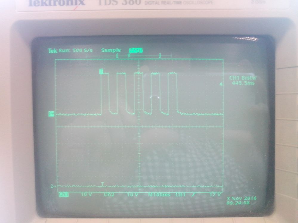
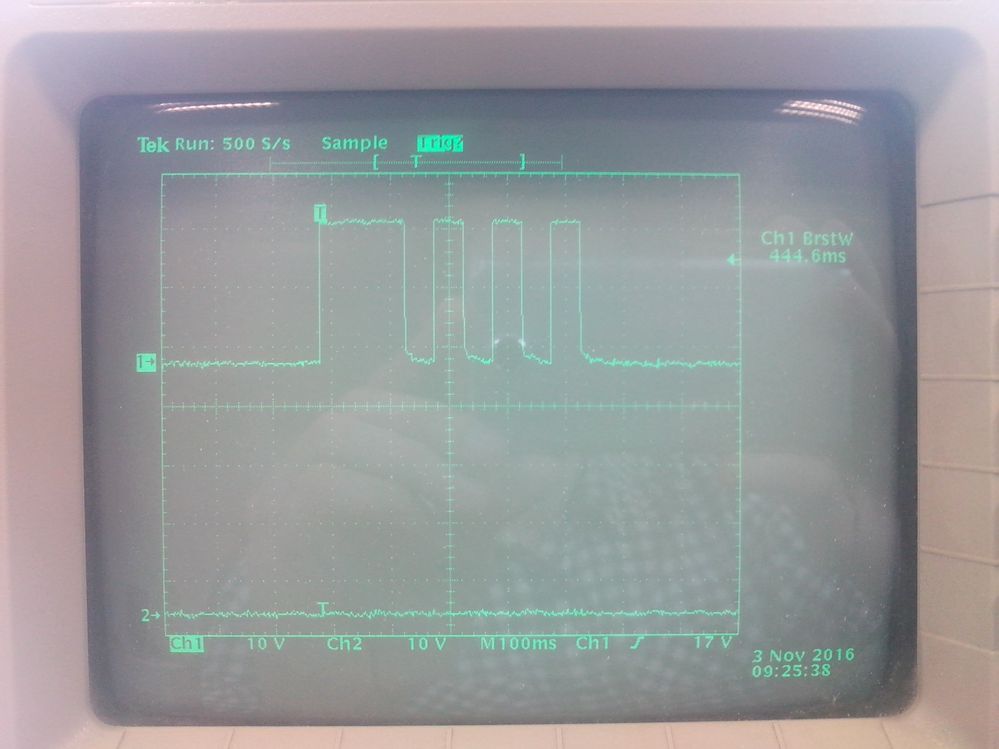
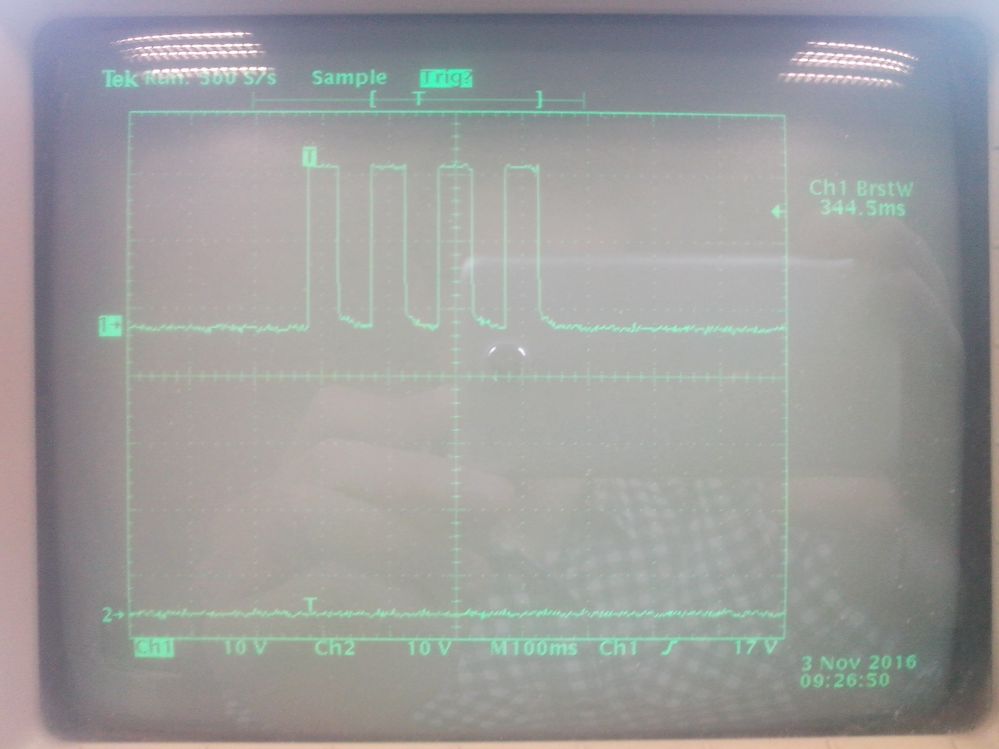
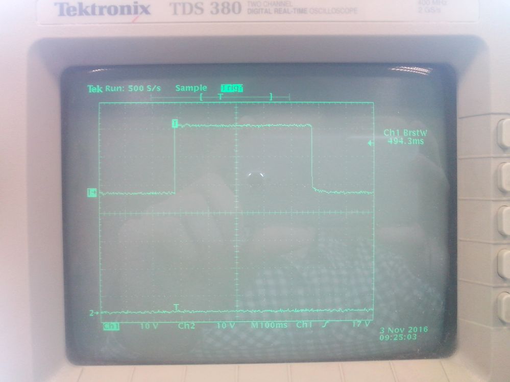
sorry for the delay, I made some screenshots of the oscilloscope output and also here is the table describing the behavior in the screenshots.
In the screenshots I always set number of pulses to 5. First screenshot shows burst sequence after previous burst sequence with DC 1% - 99% already ran. In this case number of pulses is correct = 5.
Second screenshot shows burst output when previous sequence was at 100%. In this case first two pulses are merged, so output is 1 wide + 3 narrow (normal) pulses.
Third screenshot shows burst output when previous sequence was at 0% (on scope this would be continuous low signal). In this case first pulse is skipped and only 4 pulses are output.
Fourth screenshot shows output at 100% duty cycle just for reference. I didn't attach 0% sequence since as I mentioned it's a continuous low signal.
I tried using the PWM_MatchUpdate() from PWM driver source you attached but unfortunately the result was still the same.
| Previous duty cycle | Current duty cycle | Number of pulses set | Number of pulses output |
|---|---|---|---|
| 0% | 50% | 5 | 4 |
| 1% - 99% | 50% | 5 | 5 |
| 100% | 50% | 5 | (1) + 3 |
- Mark as New
- Bookmark
- Subscribe
- Mute
- Subscribe to RSS Feed
- Permalink
- Report Inappropriate Content
Hi Marin,
I've already created a similar demo which is base on your code, and please have a try.
Have a great day,
Ping
-----------------------------------------------------------------------------------------------------------------------
Note: If this post answers your question, please click the Correct Answer button. Thank you!
-----------------------------------------------------------------------------------------------------------------------
- Mark as New
- Bookmark
- Subscribe
- Mute
- Subscribe to RSS Feed
- Permalink
- Report Inappropriate Content
Hi Martin,
Thanks for your reply, I have created the testing demo.
however I still have a query yet and hope you can clarify them.
According to your statement, the previous setting will affact next sequence PWM output, for instance skip the first PWM, merge together (100% duty),etc, so I was if you can summarize all the phenomenons in a table and share the screenshot of PWM output wave, then I can save the time for testing and focus on solving the issue and
Have a great day,
Ping
-----------------------------------------------------------------------------------------------------------------------
Note: If this post answers your question, please click the Correct Answer button. Thank you!
-----------------------------------------------------------------------------------------------------------------------


