
- Forums
- Product Forums
- General Purpose MicrocontrollersGeneral Purpose Microcontrollers
- i.MX Forumsi.MX Forums
- QorIQ Processing PlatformsQorIQ Processing Platforms
- Identification and SecurityIdentification and Security
- Power ManagementPower Management
- Wireless ConnectivityWireless Connectivity
- RFID / NFCRFID / NFC
- Advanced AnalogAdvanced Analog
- Neural Processing UnitsNeural Processing Units
- MCX Microcontrollers
- S32G
- S32K
- S32V
- MPC5xxx
- Other NXP Products
- S12 / MagniV Microcontrollers
- Powertrain and Electrification Analog Drivers
- Sensors
- Vybrid Processors
- Digital Signal Controllers
- 8-bit Microcontrollers
- ColdFire/68K Microcontrollers and Processors
- PowerQUICC Processors
- OSBDM and TBDML
- S32M
- S32Z/E
-
- Solution Forums
- Software Forums
- MCUXpresso Software and ToolsMCUXpresso Software and Tools
- CodeWarriorCodeWarrior
- MQX Software SolutionsMQX Software Solutions
- Model-Based Design Toolbox (MBDT)Model-Based Design Toolbox (MBDT)
- FreeMASTER
- eIQ Machine Learning Software
- Embedded Software and Tools Clinic
- S32 SDK
- S32 Design Studio
- GUI Guider
- Zephyr Project
- Voice Technology
- Application Software Packs
- Secure Provisioning SDK (SPSDK)
- Processor Expert Software
- Generative AI & LLMs
-
- Topics
- Mobile Robotics - Drones and RoversMobile Robotics - Drones and Rovers
- NXP Training ContentNXP Training Content
- University ProgramsUniversity Programs
- Rapid IoT
- NXP Designs
- SafeAssure-Community
- OSS Security & Maintenance
- Using Our Community
-
- Cloud Lab Forums
-
- Knowledge Bases
- ARM Microcontrollers
- i.MX Processors
- Identification and Security
- Model-Based Design Toolbox (MBDT)
- QorIQ Processing Platforms
- S32 Automotive Processing Platform
- Wireless Connectivity
- CodeWarrior
- MCUXpresso Suite of Software and Tools
- MQX Software Solutions
- RFID / NFC
- Advanced Analog
- Neural Processing Units
-
- NXP Tech Blogs
- Home
- :
- 通用微控制器
- :
- Kinetis微控制器
- :
- mcu for OpenSDA
mcu for OpenSDA

 Sabina_Bruce
Hi Javier,
In this case the K20 will still be your best option as it is inexpensive and simple, yet still provides the USB peripheral you are looking for as your referenced usb linker uses.
I'd also recommend considering utilizing the LPC-Link2 as it supports the KL05 and this programmer/debugger uses the SWD programming protocol.
For more information you can check the LPC-Link2 overview page.
I'd also recommend taking a look at the external programmers that are already made. You can find the ones recommend for the KL05 in its Tools & Software under the Emulators, Probes and Programmers.
Also, please note that any support regarding the development of the programming protocol using SWD will be with the Arm support team.
Best regards,
Sabina

Hi!
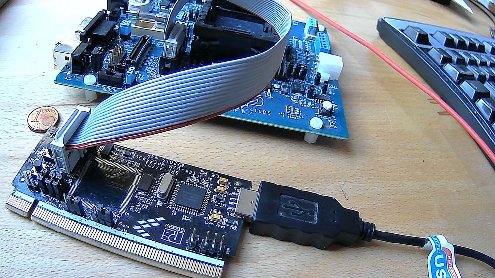
I'd like to share a similar concept for JTAG debugging with the NXP Power Architecture with you. We used to use the low budget evaluation board TRK-USB-MPC5643L as early development platform. During development, we had bricked several of the devices (seemingly due to bad debugger behavior with unprotected devices). A look into the schematics revealed that not only the pins of the JTAG connector on that board are connected to the MCU pins (for the intended purpose of debugging with an external JTAG debugger) but also the same, according set of signals from the on-board OpenSDA chip (intended for debugging over USB without additional hardware).
So why not using the JTAG connector as an output - to control another board? Only further condition: All affected pins of the MCU on the evaluation board need to be passive. Easy in our situation, we just unsoldered the bricked MCU from the boards. The wiring is a 14-wire one-by-one ribbon cable with two identical JTAG connectors at either end.
No software or configuration change is required. The debugger configuration settings in both, Code Warrior and S32 Design Studio, recognize the USB wire to the OpenSDA chip on the stripped evaluation board like they do with a P&E Multilink debugger and the same standard project settings can be used.
The solution has been tested with different boards (MPC5643L, MPC5748G and MPC5775B) and both mentioned development environments. The only perceivable difference to a true P&E Multilink is the a bit lower data transmission speed during flashing.
 Sabina_Bruce
Hello Javier,
Firstly you need to define and consider what your target MCU is, because this will help you determine what MCU you may use as debug probe and consequently if it will be with OpenSDA or other SWD or JTAG protocols.
Since debug probes are usually connected to your host workstation via USB, the K20 is the simplest choice that still has a USB peripheral.
Let me know if you have further questions.
Best Regards,
Sabina
Sabina_Bruce
Hello Javier,
Due to the nature of the OpenSDA, the Kinetis K20 is the best choice for price and simplicity. In addition the OpenSDA was designed to function correctly only with the K20.
Also, from the description of what you are trying to achieve I understand you'd like to make a programmer/debugger using OpenSDA. The link that you provided is not a debugger this device has a different purpose, than what your intending to do with the K20.
Best Regards,
Sabina
Hello Sabina,
Yes, you are in the right. I don't want to debug the KL05, I want flash the firmware and read/write.
The other systems use a FTDI + Arduino ISP programmer in order to flash de firmware in the target. I want to made some similar in only one device.
Best regards
Sabina_Bruce
Hi Javier,
In this case the K20 will still be your best option as it is inexpensive and simple, yet still provides the USB peripheral you are looking for as your referenced usb linker uses.
I'd also recommend considering utilizing the LPC-Link2 as it supports the KL05 and this programmer/debugger uses the SWD programming protocol.
For more information you can check the LPC-Link2 overview page.
I'd also recommend taking a look at the external programmers that are already made. You can find the ones recommend for the KL05 in its Tools & Software under the Emulators, Probes and Programmers.
Also, please note that any support regarding the development of the programming protocol using SWD will be with the Arm support team.
Best regards,
Sabina

I don't see anything in the tools and software section that does anything close to what he wants to do. I only see the PE multilink programmers or development boards. What he wants to do (i think) is take the OpenSDA portion of the dev boards and make it standalone. I've been looking for this as well. I'm not sure why NXP doesn't offer this.
jhd have you made any progress? I'm going give it a shot myself I guess.
No, I'm was working in a open 32 bits esc with rgb led with kl05/04. It's finished but not sure that I goes to work in this now but I need it.
I only need the device to program and debugger the esc and other devices as the vtx (kl03). Like as the Erich is ok to me I think.

Not sure if you have seen the tinyK20 we did at the Lucerne University:
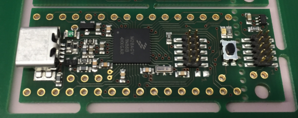
tinyK20 Open Source ARM Debug/Universal Board – First Prototypes | MCU on Eclipse
tinyK20: New Board with micro-SD Card | MCU on Eclipse
Production tinyK20 Boards arrived! | MCU on Eclipse
It is basically using the OpenSDA circuit from the FRDM boards, but can be used as standalone breakout board (main purpose) or as a board to debug other Kinetis devices using CMSIS-DAP. It is using the same K20DX128 as on the FRDM boards: that way it is binary compatible to it.
We looked at using a differnt MCU, but this was not really feasible:
- price was rather high because of small number of boards. Our batches were in the 100-200 range to equip students with breakout boards.
- using a different microcontroller would require to port the bootloader. But because the OpenSDA 2.0+ bootloader needs using proprietary and expensive tools (see Adding a Delay to the ARM DAPLink Bootloader | MCU on Eclipse ) plus would need extra efforts we did not consider that option.
With that small number of boards, the BOM of the K20 including assembly (without any cables) was around $20.
So for us using the K20 was a good choice and has worked out very well. Later versions of a similar board have the K20 embedded on the board too: First tinyK22 Board with NXP K22FN512 ARM Cortex-M4F | MCU on Eclipse
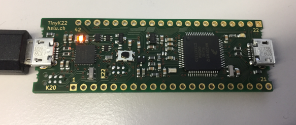
If anywone would be interested to invest money and produce a large batch of boards to get the costs down, this could be considered of course. Ping me directly and I can see if there is any interest :-).
I hope this helps,
Erich
This seems to be what I'm talking about, thank you for sharing! I can't tell if the K22 is an updated version or something more different. You're obviously using it as more than just a programmer/debugger, which is great, but it's muddying the waters for me a bit. I'm new to the ARM processor and OpenSDA.
What I'm trying to do is pull the OpenSDA portion of the dev board off and use it in exactly the same way it's currently being used. I want to build a custom PCB based on ARM M4 and use the K20 board to program it using OpenSDA. That way I don't have to build an elaborate OpenSDA circuit into my production boards.
Is that something that your board can do? Thanks again!
Dylan
Hi Dylan,
yes, this is exactly what the tinyK20 is able to do.
On the tinyK22 the OpenSDA circuit is embedded on the board as it is for example on the FRDM-K22F board.
In case you are not aware: you can use an existing board (e.g. see Using the Freescale Freedom (FRDM-KL43Z) to Debug other Boards | MCU on Eclipse) to debug another one. It depends a bit on the board, but in most cases you need to add a jumper/cut a trace and add a header.
An even better and less expensive way is using the LPC845-BRK for this:
Tutorial: Transforming the NXP LPC845-BRK into a CMSIS-DAP Debug Probe | MCU on Eclipse
For $5 you have a development board and a debug probe:
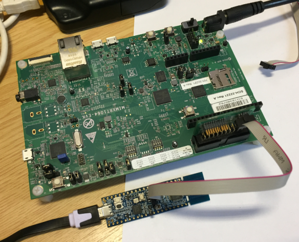
or see Using the LPCXpresso V2/V3 Boards to Debug an external Board | MCU on Eclipse .
Just one word on this: all these options are low cost options, so don't expect ultra fast debugging or flash programming. A Segger J-Link, LPC-Link2 or P&E Multilink are much more convenient to use and fasters by factors.
You can get a J-LINK EDU for $20, or a LPC-Link2 (if you are not aware of it) for $20 too (see Custom 3D Printed Enclosure for NXP LPC-Link2 Debug Probes | MCU on Eclipse ). I really recommend to invest at least that money.
I hope this helps,
Erich
Well it seems like there are many solutions to my problem, thank you for the wealth of information. Money is not an issue so I definitely want to get something decent, however, after reading through your articles I went back to the schematic for the S32K144EVB and it looks like it can also be used as a programmer/debugger for external boards.
One thing I didn't mention earlier is that I'm developing in Simulink and the OpenSDA interface allows me to build and program in Simulink rather than using a traditional IDE. This is literally my first NXP/ARM project so pardon my ignorance but I wasn't sure that a "regular" programmer would work with Simulink or if NXP had done something under the hood to work with the OpenSDA on the dev boards. I don't even know what CMSIS-DAP is, for instance :-). I have some research to do!
At any rate, you've been very helpful and I think I have enough information to move down the road with my design knowing that I will be able to program it when it arrives! Love your blog, I've got it bookmarked for future reading.
Dylan
