- Forums
- Product Forums
- General Purpose MicrocontrollersGeneral Purpose Microcontrollers
- i.MX Forumsi.MX Forums
- QorIQ Processing PlatformsQorIQ Processing Platforms
- Identification and SecurityIdentification and Security
- Power ManagementPower Management
- Wireless ConnectivityWireless Connectivity
- RFID / NFCRFID / NFC
- Advanced AnalogAdvanced Analog
- MCX Microcontrollers
- S32G
- S32K
- S32V
- MPC5xxx
- Other NXP Products
- S12 / MagniV Microcontrollers
- Powertrain and Electrification Analog Drivers
- Sensors
- Vybrid Processors
- Digital Signal Controllers
- 8-bit Microcontrollers
- ColdFire/68K Microcontrollers and Processors
- PowerQUICC Processors
- OSBDM and TBDML
- S32M
- S32Z/E
-
- Solution Forums
- Software Forums
- MCUXpresso Software and ToolsMCUXpresso Software and Tools
- CodeWarriorCodeWarrior
- MQX Software SolutionsMQX Software Solutions
- Model-Based Design Toolbox (MBDT)Model-Based Design Toolbox (MBDT)
- FreeMASTER
- eIQ Machine Learning Software
- Embedded Software and Tools Clinic
- S32 SDK
- S32 Design Studio
- GUI Guider
- Zephyr Project
- Voice Technology
- Application Software Packs
- Secure Provisioning SDK (SPSDK)
- Processor Expert Software
- Generative AI & LLMs
-
- Topics
- Mobile Robotics - Drones and RoversMobile Robotics - Drones and Rovers
- NXP Training ContentNXP Training Content
- University ProgramsUniversity Programs
- Rapid IoT
- NXP Designs
- SafeAssure-Community
- OSS Security & Maintenance
- Using Our Community
-
- Cloud Lab Forums
-
- Knowledge Bases
- ARM Microcontrollers
- i.MX Processors
- Identification and Security
- Model-Based Design Toolbox (MBDT)
- QorIQ Processing Platforms
- S32 Automotive Processing Platform
- Wireless Connectivity
- CodeWarrior
- MCUXpresso Suite of Software and Tools
- MQX Software Solutions
- RFID / NFC
- Advanced Analog
-
- NXP Tech Blogs
- Home
- :
- 通用微控制器
- :
- Kinetis微控制器
- :
- Re: flexram to eep
flexram to eep
I want to use flexram to eep!
MY CPU IS MK60FX512VLQ15,
1,what is D-FLAS 0 IFR abs address ? CAN I read it from IAR debug?
2,How many bytes about 1 Flash Block,1 Flash Section,where to set it?
3,when I earse one Flash Section ,how many byte I earsed ? earsing start address is setted by FTFE_FCCOB1,FTFE_FCCOB2,FTFE_FCCOB3?
已解决! 转到解答。
Hi 何胜利,
Please kindly refer to the following answer for your question:
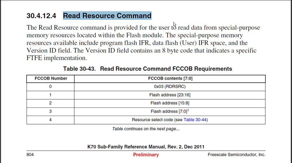
1,what is D-FLAS 0 IFR abs address ? CAN I read it from IAR debug?
-D-FLAS 0 IFR can only be accessed by Read Resource Command, please refer to the following for details.
2,How many bytes about 1 Flash Block,1 Flash Section,where to set it?
-Do you mean flash section instead of flash section? Actually the size of flash block and sector are determined by device, no register can be used to configure them on the fly. Please kindly refer to Chapter 3 Chip Configuration in RM for details. You may find something like below:
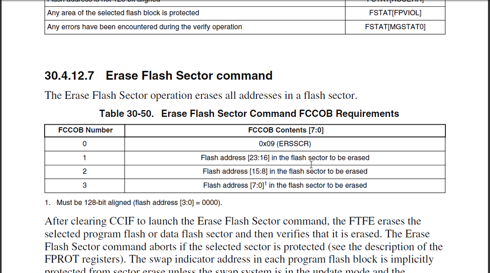
3,when I earse one Flash Section ,how many byte I earsed ? earsing start address is setted by FTFE_FCCOB1,FTFE_FCCOB2,FTFE_FCCOB3?
-Do you mean erasing Flash sector command? Then the bytes to be erased is size of a sector, for example, 4KB. and yes, earsing start address is setted by FTFE_FCCOB1,FTFE_FCCOB2,FTFE_FCCOB3. Please refer to the following for more details.
Hope that helps,
Have a great day,
Kan
-----------------------------------------------------------------------------------------------------------------------
Note: If this post answers your question, please click the Correct Answer button. Thank you!
-----------------------------------------------------------------------------------------------------------------------


