- Forums
- Product Forums
- General Purpose MicrocontrollersGeneral Purpose Microcontrollers
- i.MX Forumsi.MX Forums
- QorIQ Processing PlatformsQorIQ Processing Platforms
- Identification and SecurityIdentification and Security
- Power ManagementPower Management
- Wireless ConnectivityWireless Connectivity
- RFID / NFCRFID / NFC
- Advanced AnalogAdvanced Analog
- MCX Microcontrollers
- S32G
- S32K
- S32V
- MPC5xxx
- Other NXP Products
- S12 / MagniV Microcontrollers
- Powertrain and Electrification Analog Drivers
- Sensors
- Vybrid Processors
- Digital Signal Controllers
- 8-bit Microcontrollers
- ColdFire/68K Microcontrollers and Processors
- PowerQUICC Processors
- OSBDM and TBDML
- S32M
- S32Z/E
-
- Solution Forums
- Software Forums
- MCUXpresso Software and ToolsMCUXpresso Software and Tools
- CodeWarriorCodeWarrior
- MQX Software SolutionsMQX Software Solutions
- Model-Based Design Toolbox (MBDT)Model-Based Design Toolbox (MBDT)
- FreeMASTER
- eIQ Machine Learning Software
- Embedded Software and Tools Clinic
- S32 SDK
- S32 Design Studio
- GUI Guider
- Zephyr Project
- Voice Technology
- Application Software Packs
- Secure Provisioning SDK (SPSDK)
- Processor Expert Software
- Generative AI & LLMs
-
- Topics
- Mobile Robotics - Drones and RoversMobile Robotics - Drones and Rovers
- NXP Training ContentNXP Training Content
- University ProgramsUniversity Programs
- Rapid IoT
- NXP Designs
- SafeAssure-Community
- OSS Security & Maintenance
- Using Our Community
-
- Cloud Lab Forums
-
- Knowledge Bases
- ARM Microcontrollers
- i.MX Processors
- Identification and Security
- Model-Based Design Toolbox (MBDT)
- QorIQ Processing Platforms
- S32 Automotive Processing Platform
- Wireless Connectivity
- CodeWarrior
- MCUXpresso Suite of Software and Tools
- MQX Software Solutions
- RFID / NFC
- Advanced Analog
-
- NXP Tech Blogs
- Home
- :
- 通用微控制器
- :
- Kinetis微控制器
- :
- What pins are used to program and debug the kl2x series
What pins are used to program and debug the kl2x series
What pins are used to program and debug the kl2x series
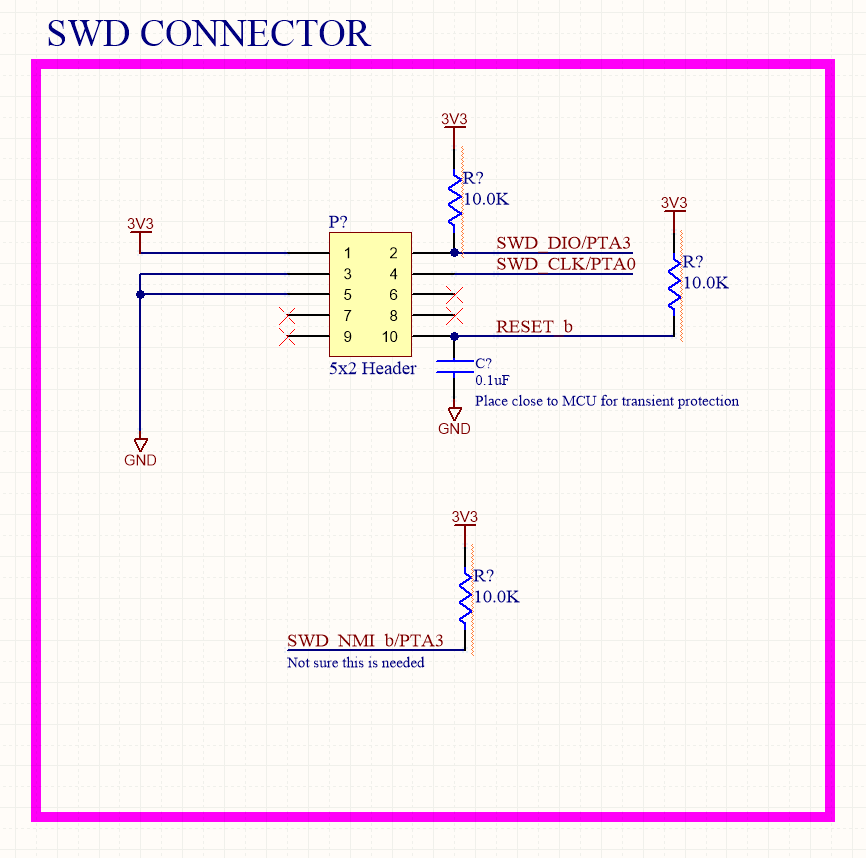
I have researched the decided that I would like to use the KL24 in my newest design. I have created most of the schematic but it missing on how to load code onto it. I have never used the KL2x series microcontrollers before and I am not sure what lines are used to connect a JTAG programmer to.
Do I load my code directly via the USB connection?
How do I debug my code?
Complete part number that I intend to use is MKL24Z32VFM4.
Hi Lance Robbins,
Here is the SWD debug port for Kinetis L series.
You also need to pay attention to the connection of 'RESET_b and NMI_b'.
Kinetis L Peripheral Module Quick Reference is recommend for you to read.
Best Regards,
Robin
-----------------------------------------------------------------------------------------------------------------------
Note: If this post answers your question, please click the Correct Answer button. Thank you!
-----------------------------------------------------------------------------------------------------------------------
Thank you Mark and Robin,
Below is what I got from your input. I wasn't sure what to do with the NMI_b pin so i tied it to 3V3 through a pull-up.
In my application I will not need a push button reset button as shown in FRDM-KL25Z_SCH_REV_E.pdf.
My circuit is low power and I plan on using the KL24 internal USB Voltage regulator to generate 3V3. It normal operating current should be around 20mA not counting what the KL24 microcontroller uses.
If you see a problem please let me know.
Thanks very much,
Lance
External Capacitor should be connected with Pin VOUT33.
With the low-power mode, the oscillator has the internal feedback resistor RF. Therefore, the feedback resistor must not be
externally with the Connection 3.
Best Regards,
Robin
-----------------------------------------------------------------------------------------------------------------------
Note: If this post answers your question, please click the Correct Answer button. Thank you!
-----------------------------------------------------------------------------------------------------------------------
Hi
The KL24 doesn't have JTAG - it has SWD.
Copy the SWD connection circuit from the FRDM-KL25Z diagram: https://www.nxp.com/downloads/en/schematics/FRDM-KL25Z_SCH_REV_E.pdf
There is no ROM loader in the KL24 so you need a debugger (eg. J-Link or P&E) to program it. Code debugging can be done with the same tool using a variety of IDEs - KDS is suitable.
Regards
Mark
Kinetis: http://www.utasker.com/kinetis.html
KL25:
- http://www.utasker.com/kinetis/FRDM-KL25Z.html
- http://www.utasker.com/kinetis/TWR-KL25Z48M.html
- http://www.utasker.com/kinetis/RD-KL25-AGMP01.html


