Understanding ADC specifications
Although most of us have a basic understanding of how an ADC works and how to understand some of the basic figures that define an ADC performance, that is far from really understanding how to fully interpret and use the figures depicted in a datasheet ADC section. With all those numbers it is easy to get lost on which ones to look at when we want to know how it will react to conditions such as frequency, signal amplitude, temperature, etc; having such knowledge would allow us to better fit a specific ADC to your application and take full advantage of its features.
Having this in mind I took the time to compile some information related to what the most common figures that describe an ADC performance depicted in a datasheet mean, most of the material can be found in any Analog to Digital Conversion theory book; as I mentioned before this is just a general compilation of knowledge I hope will help you better understand those specifications. It assumes those of us who use datasheets are somehow familiar with the basic working of ADCs, so I will spare the basic concepts.
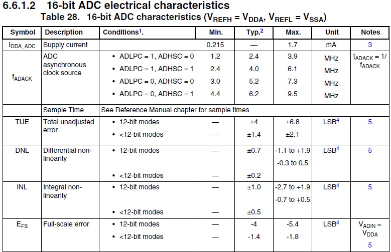
Now down to business, this is a extract of a typical ADC section from a microcontroller's datasheet:
I am almost certain not a lot of people who use microcontrollers, and more specifically ADCs; have a clear idea of what Total Unadjusted Error, Integral Non-Linearity or Differential Non-Linearity describe in the behavior of an ADC. Even though I will try to describe in detail the most common parameters I might miss some others and there is the possibility some of the information might not be as accurate as I would like it to be, if any of you reading this brief document have specific questions regarding any parameter I describe or miss by all means comment.
Common ADC electrical characteristics depicted in datasheets
- EQ Quantization error
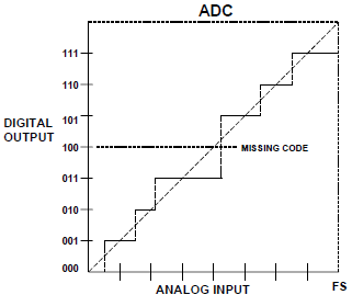
Since the analog input to an ADC can take any value, but the digital output is quantized, there may be a difference of up to ½ Less Significant Bit between the actual analog input and the exact value of the digital output. This is known as the quantization error or quantization uncertainty as shown below. In ac (sampling) applications this quantization error gives rise to quantization noise.
- SINAD, SNR and ENOB (Signal to Noise plus Distortion, SIgnal to Noise Ratio and Effective Number of Bits)
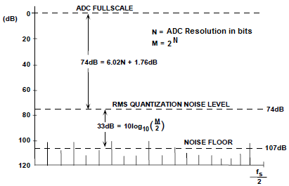
Signal-to-Noise-and Distortion (SINAD, or S/(N + D) is the ratio of the rms signal amplitude to the mean value of the root-sum square (rss) of all other spectral components, including harmonics, but excluding dc. SINAD is a good indication of the overall dynamic performance of an ADC as a function of input frequency because it includes all components which make up noise (including thermal noise) and distortion. It is often plotted for various input amplitudes. SINAD is equal to THD + N if the bandwidth for the noise measurement is the same. SINAD is often converted to effective-number-of-bits (ENOB) using the relationship for the theoretical SNR of an ideal N-bit ADC: SNR = 6.02N + 1.76 dB, the equation is solved for N, and the value of SINAD is substituted for SNR.
Effective number of bits (ENOB) is a measure of the dynamic performance of an analog to digital converter and its associated circuitry. The resolution of an ADC is specified by the number of bits used to represent the analog value, in principle giving 2N signal levels for an N-bit signal. However, all real ADC circuits introduce noise and distortion. ENOB specifies the resolution of an ideal ADC circuit that would have the same resolution as the circuit under consideration. Often ENOB is calculated using the relationship for the theoretical SNR of an ideal N-bit ADC: SNR = 6.02N + 1.76 dB, the equation is solved for N, and the value of SINAD is substituted for SNR.
- SFDR Spurious Free Dynamic Range
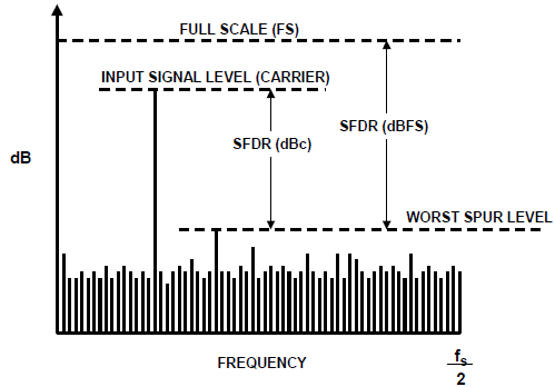
One of the most significant specification for an ADC used in a communications application is its spurious free dynamic range (SFDR). SFDR of an ADC is defined as the ratio of the rms signal amplitude to the rms value of the peak spurious spectral content measured over the bandwidth of interest. SFDR is generally plotted as a function of signal amplitude and may be expressed relative to the signal amplitude (dBc) or the ADC full-scale (dBFS) as shown in Figure n. For a signal near full-scale, the peak spectral spur is generally determined by one of the first few harmonics of the fundamental. However, as the signal falls several dB below full-scale, other spurs generally occur which are not direct harmonics of the input signal. This is because of the differential nonlinearity of the ADC transfer function as discussed earlier. Therefore, SFDR considers all sources of distortion, regardless of their origin.
- INL Integral Non-Linearity
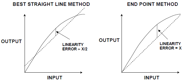
Integral nonlinearity (acronym INL) is the maximum deviation between the ideal output of an ADC and the actual output level (after offset and gain errors have been removed). The transfer function of an ADC should ideally be a line and the INL measurement depends on the ideal line selected. Two often used lines are the best fit line, which is the line that minimizes the INL result and the endpoint line which is a line that passes through the points on the transfer function corresponding to the lowest and highest input code. In all cases, the INL is the maximum distance between the ideal line selected and the actual transfer function.
- DNL Differential Non-Linearity
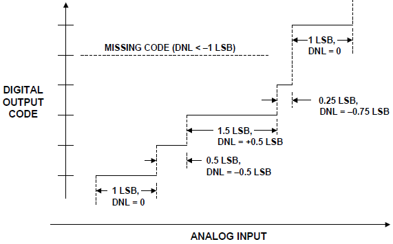
Differnetial NonLinearity relates to the linearity of the code transitions of the converter. In the ideal case, a change of 1 LSB in digital code corresponds to a change of exactly 1 LSB of analog signal. In an ADC there should be exactly 1 LSB change of analog input to move from one digital transition to the next. Differential linearity error is defined as the maximum amount of deviation of any quantum (or LSB change) in the entire transfer function from its ideal size of 1 LSB. Where the change in analog signal corresponding to 1 LSB digital change is more or less than 1 LSB, there is said to be a DNL error. The DNL error of a converter is normally defined as the maximum value of DNL to be found at any transition across the range of the converter. The following figure shows the non-ideal transfer functions for an ADC and shows the effects of the DNL error.
A common result of excess DNL in ADCs is missing codes resulting from DNL < –1 LSB.
- THD Total Harmonic Distortion
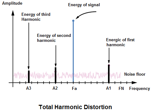
Total harmonic distortion (THD) is the ratio of the rms value of the fundamental signal to the mean value of the root-sum-square of its harmonics (generally, only the first 5 are significant). THD of an ADC is also generally specified with the input signal close to full-scale, the harmonics of the input signal can be distinguished from other distortion by their location in the frequency spectrum. The second and third harmonics are generally the only ones specified on a data sheet because they tend to be the largest.
- EFS Full Scale Error
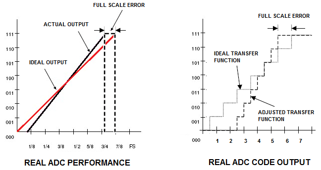
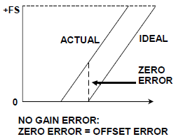
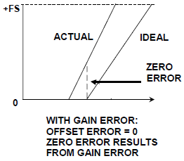
Full-scale error can be defined as the difference between the actual value triggering the transition to full-scale and the ideal analog full-scale transition value. Full-scale error is equal to the offset error + gain error
Offset error
The transfer characteristics of both DACs and ADCs may be expressed as a straight line
given by D = K + GA, where D is the digital code, A is the analog signal, and K and G
are constants. In a unipolar converter, the ideal value of K is zero. The offset error is the
amount by which the actual value of K differs from its ideal value.
Gain error
The gain error is the amount by which G differs from its ideal value, and is generally
expressed as the percentage difference between the two, although it may be defined as
the gain error contribution (in mV or LSB) to the total error at full-scale.
- TUE Total Unadjusted Error
This is the result of performing conversions without having calibrated the ADC, it is dominated by the uncalibrated gain and uncalibrated offset terms in the data sheet. Although most devices will be well within the data sheet limits, it should be noted that they are not centered around zero and full range of the incoming analog signal is not guaranteed. Therefore, an uncalibrated ADC will always show unknown levels of gain and offset error, thus reflecting the worst case of conversion error the module can provide.
I have a question about these ADC specifications. It is a 16 bit ADC, but why are specifications for DNL and INL given for 12 bit modes and < 12 bit modes? It seems like specifications for the 16 bit mode are not given in this table, and those are what I am most curious about. (I am using a KL16, and am considering moving to the KL17).
