- Forums
- Product Forums
- General Purpose MicrocontrollersGeneral Purpose Microcontrollers
- i.MX Forumsi.MX Forums
- QorIQ Processing PlatformsQorIQ Processing Platforms
- Identification and SecurityIdentification and Security
- Power ManagementPower Management
- Wireless ConnectivityWireless Connectivity
- RFID / NFCRFID / NFC
- Advanced AnalogAdvanced Analog
- MCX Microcontrollers
- S32G
- S32K
- S32V
- MPC5xxx
- Other NXP Products
- S12 / MagniV Microcontrollers
- Powertrain and Electrification Analog Drivers
- Sensors
- Vybrid Processors
- Digital Signal Controllers
- 8-bit Microcontrollers
- ColdFire/68K Microcontrollers and Processors
- PowerQUICC Processors
- OSBDM and TBDML
- S32M
- S32Z/E
-
- Solution Forums
- Software Forums
- MCUXpresso Software and ToolsMCUXpresso Software and Tools
- CodeWarriorCodeWarrior
- MQX Software SolutionsMQX Software Solutions
- Model-Based Design Toolbox (MBDT)Model-Based Design Toolbox (MBDT)
- FreeMASTER
- eIQ Machine Learning Software
- Embedded Software and Tools Clinic
- S32 SDK
- S32 Design Studio
- GUI Guider
- Zephyr Project
- Voice Technology
- Application Software Packs
- Secure Provisioning SDK (SPSDK)
- Processor Expert Software
- Generative AI & LLMs
-
- Topics
- Mobile Robotics - Drones and RoversMobile Robotics - Drones and Rovers
- NXP Training ContentNXP Training Content
- University ProgramsUniversity Programs
- Rapid IoT
- NXP Designs
- SafeAssure-Community
- OSS Security & Maintenance
- Using Our Community
-
- Cloud Lab Forums
-
- Knowledge Bases
- ARM Microcontrollers
- i.MX Processors
- Identification and Security
- Model-Based Design Toolbox (MBDT)
- QorIQ Processing Platforms
- S32 Automotive Processing Platform
- Wireless Connectivity
- CodeWarrior
- MCUXpresso Suite of Software and Tools
- MQX Software Solutions
- RFID / NFC
- Advanced Analog
-
- NXP Tech Blogs
- Home
- :
- 汎用マイクロコントローラ
- :
- Kinetisマイクロコントローラ
- :
- Unable to debug MK22FN1M0VLH12
Unable to debug MK22FN1M0VLH12
- RSS フィードを購読する
- トピックを新着としてマーク
- トピックを既読としてマーク
- このトピックを現在のユーザーにフロートします
- ブックマーク
- 購読
- ミュート
- 印刷用ページ
- 新着としてマーク
- ブックマーク
- 購読
- ミュート
- RSS フィードを購読する
- ハイライト
- 印刷
- 不適切なコンテンツを報告
Right now i am unable to program or debug MK22FN1M0VLH12 by using swd of j-link. I often use j-link swd to debug K60, so i am sure it is not a connection or schematic problem.
When i look at the waveform of reset pin, i found the reset pin to be oscillating. Please help me find a way to program the MCU, as i have already made the PCB with swd connection.
解決済! 解決策の投稿を見る。
- 新着としてマーク
- ブックマーク
- 購読
- ミュート
- RSS フィードを購読する
- ハイライト
- 印刷
- 不適切なコンテンツを報告
Hi Handy,
I have a couple of things to check and hopefully this helps.
1) Make sure that you have the right part selected in your IDE tool and make sure you are using the correct flashloader. What tool are you using? And are you not even able to connect with downloading?
2) Is this only your project that you are having trouble with? Have you tried using the Freescale provided sample code associated with this part? If it will not download, can you send me the link where you got the sample code just so that I know exactly what you are looking at?
3) Can you check the voltage on PTA4? It should be high, but I want to be sure. If it is not, that could be the issue.
Hope this helps,
Chris
- 新着としてマーク
- ブックマーク
- 購読
- ミュート
- RSS フィードを購読する
- ハイライト
- 印刷
- 不適切なコンテンツを報告
I suppose the problem lies in incorrect setting of IDE or debugger. Right now i could debug every K22 that i have. I am unable to recreate the same problem that i have before.
- 新着としてマーク
- ブックマーク
- 購読
- ミュート
- RSS フィードを購読する
- ハイライト
- 印刷
- 不適切なコンテンツを報告
Hi Handy,
I have a couple of things to check and hopefully this helps.
1) Make sure that you have the right part selected in your IDE tool and make sure you are using the correct flashloader. What tool are you using? And are you not even able to connect with downloading?
2) Is this only your project that you are having trouble with? Have you tried using the Freescale provided sample code associated with this part? If it will not download, can you send me the link where you got the sample code just so that I know exactly what you are looking at?
3) Can you check the voltage on PTA4? It should be high, but I want to be sure. If it is not, that could be the issue.
Hope this helps,
Chris
- 新着としてマーク
- ブックマーク
- 購読
- ミュート
- RSS フィードを購読する
- ハイライト
- 印刷
- 不適切なコンテンツを報告
Hello Handy Chandra:
The reset pin oscillating is expected in new/unprogrammed parts.
Can you show the SWD connection schematics? SWD_DIO line must have a pull up.
For more ideas regarding this connection problem give a check to the next thread:
PE multilink JTAG/BDM Kinetis programming issue
Regards!,
Jorge Gonzalez
-----------------------------------------------------------------------------------------------------------------------
Note: If this post answers your question, please click the Correct Answer button. Thank you!
-----------------------------------------------------------------------------------------------------------------------
- 新着としてマーク
- ブックマーク
- 購読
- ミュート
- RSS フィードを購読する
- ハイライト
- 印刷
- 不適切なコンテンツを報告
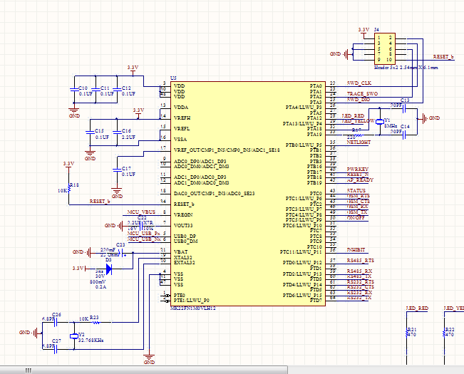
Here is the schematic of SWD Connection. I have tried adding pullup on SWD_DIO and pulldown on SWD_CLK on the PCB, but it is still not working.
None of the methods on your link earlier worked either.
- 新着としてマーク
- ブックマーク
- 購読
- ミュート
- RSS フィードを購読する
- ハイライト
- 印刷
- 不適切なコンテンツを報告
Hi Handy,
Could you tried to use J-Link tool debug your designed K22 board? Could not work?
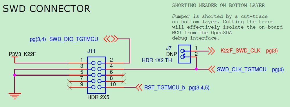
Below is FRDM-K22F120 board SWD interface schematics for your reference:
Wish it helps.
best regards
Ma Hui
-----------------------------------------------------------------------------------------------------------------------
Note: If this post answers your question, please click the Correct Answer button. Thank you!
-----------------------------------------------------------------------------------------------------------------------
- 新着としてマーク
- ブックマーク
- 購読
- ミュート
- RSS フィードを購読する
- ハイライト
- 印刷
- 不適切なコンテンツを報告
Hi Ma Hui,
Yes, the swd connection is about the same, except for pin 9 connected to gnd and pin 6 connected to tdo.
I have tried two mcu and both of them fail at debugging. Yesterday, i tried the third mcu, and suddenly i could debug it !. I don't know what went wrong with the first two. The pcb is still the same with the same connection with pullup on dio and pulldown on clk.
- 新着としてマーク
- ブックマーク
- 購読
- ミュート
- RSS フィードを購読する
- ハイライト
- 印刷
- 不適切なコンテンツを報告
It looks like some electron noise affect SWD communication. So customer could consider to add 10uF bypass capacitor to K22 VDD power line.
Wish it helps.
best regards
Ma Hui
-----------------------------------------------------------------------------------------------------------------------
Note: If this post answers your question, please click the Correct Answer button. Thank you!
-----------------------------------------------------------------------------------------------------------------------

