- Forums
- Product Forums
- General Purpose MicrocontrollersGeneral Purpose Microcontrollers
- i.MX Forumsi.MX Forums
- QorIQ Processing PlatformsQorIQ Processing Platforms
- Identification and SecurityIdentification and Security
- Power ManagementPower Management
- Wireless ConnectivityWireless Connectivity
- RFID / NFCRFID / NFC
- Advanced AnalogAdvanced Analog
- MCX Microcontrollers
- S32G
- S32K
- S32V
- MPC5xxx
- Other NXP Products
- S12 / MagniV Microcontrollers
- Powertrain and Electrification Analog Drivers
- Sensors
- Vybrid Processors
- Digital Signal Controllers
- 8-bit Microcontrollers
- ColdFire/68K Microcontrollers and Processors
- PowerQUICC Processors
- OSBDM and TBDML
- S32M
- S32Z/E
-
- Solution Forums
- Software Forums
- MCUXpresso Software and ToolsMCUXpresso Software and Tools
- CodeWarriorCodeWarrior
- MQX Software SolutionsMQX Software Solutions
- Model-Based Design Toolbox (MBDT)Model-Based Design Toolbox (MBDT)
- FreeMASTER
- eIQ Machine Learning Software
- Embedded Software and Tools Clinic
- S32 SDK
- S32 Design Studio
- GUI Guider
- Zephyr Project
- Voice Technology
- Application Software Packs
- Secure Provisioning SDK (SPSDK)
- Processor Expert Software
- Generative AI & LLMs
-
- Topics
- Mobile Robotics - Drones and RoversMobile Robotics - Drones and Rovers
- NXP Training ContentNXP Training Content
- University ProgramsUniversity Programs
- Rapid IoT
- NXP Designs
- SafeAssure-Community
- OSS Security & Maintenance
- Using Our Community
-
- Cloud Lab Forums
-
- Knowledge Bases
- ARM Microcontrollers
- i.MX Processors
- Identification and Security
- Model-Based Design Toolbox (MBDT)
- QorIQ Processing Platforms
- S32 Automotive Processing Platform
- Wireless Connectivity
- CodeWarrior
- MCUXpresso Suite of Software and Tools
- MQX Software Solutions
- RFID / NFC
- Advanced Analog
-
- NXP Tech Blogs
- Home
- :
- General Purpose Microcontrollers
- :
- Kinetis Microcontrollers
- :
- SDRAM cache and benchmarking on K65
SDRAM cache and benchmarking on K65
- Subscribe to RSS Feed
- Mark Topic as New
- Mark Topic as Read
- Float this Topic for Current User
- Bookmark
- Subscribe
- Mute
- Printer Friendly Page
- Mark as New
- Bookmark
- Subscribe
- Mute
- Subscribe to RSS Feed
- Permalink
- Report Inappropriate Content
Hi,
Marek Neuzil was kind enough to provide a working SDRAM example for Processor Expert. He posted it here: Re: can't read data back from SDRAM.
I modified it slightly to get some time measurement into it for better benchmarking of the SDRAM performance.
Unfortunetly, the numbers I get are worse than expected.
I'm getting arround 57 MB/s of memset performance.
I would expect something that is derived from a theoretical value of 240 MB/s (60 MHz bus clock x 32 Bit Buswidth)
Solved! Go to Solution.
- Mark as New
- Bookmark
- Subscribe
- Mute
- Subscribe to RSS Feed
- Permalink
- Report Inappropriate Content
Peter,
The system bus is used for all accesses to addresses between 0x2000_0000-0xDFFF_FFFF and 0xE010_0000-0xFFFF_FFFF by the Core. Therefore the system cache can be used for caching of SDRAM data that are accessed by using 0x7000_0000–0x7FFF_FFFF or 0x8000_0000–0x8FFF_FFFF addresses (R7 and R8 cache regions).
Best Regards,
Marek Neuzil
- Mark as New
- Bookmark
- Subscribe
- Mute
- Subscribe to RSS Feed
- Permalink
- Report Inappropriate Content
I somehow messed up the initla post and want to share the KDS project I am using.
part of my concern is also, that L1 cache does net seem to have any influence on SDRAM performance.
SDRAM is accessed at the location of 0x70000000 which is a set as cachable region (write-back) by default. But turning LMEM cache on, does not influence the numbers I'm getting....
can anyone reproduce my findings ?
- Mark as New
- Bookmark
- Subscribe
- Mute
- Subscribe to RSS Feed
- Permalink
- Report Inappropriate Content
...please... anyone ?
- Mark as New
- Bookmark
- Subscribe
- Mute
- Subscribe to RSS Feed
- Permalink
- Report Inappropriate Content
Hello Peter,
I have checked your K65 benchmark application and I have also modified the write access by using eDMA (highest priority for the eDMA in the AXBS). But the performance is the same.
It seems that 57MB/s is the maximum for the SDRAM that is available on the K65 tower board.
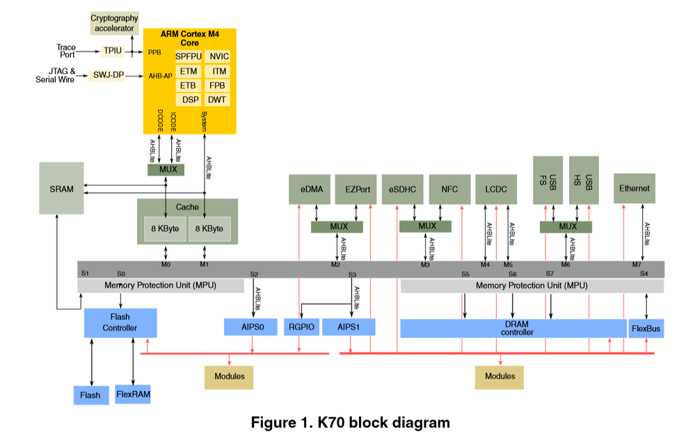
Please, look at the block diagram of the Kinetis K-series (ARM Cortex M4), e.g. K70 block diagram:
The SDRAM memory chip is connected to the SDRAM (DRAM) controller of the MCU. The SDRAM controller is connected to a slave port of the Crossbar (internal bus), i.e. there is not direct access from CPU (or eDMA) to SDRAM, there must be always request to SDRAM controller that provides access to SDRAM memory without any cache. There is always delay to read/write data from/to SDRAM. In addition, there is always sequence of reading/writing data (ACTV, NOP, READ/WRITE, PALL) and refresh operations. Therefore the performance cannot be near to bus_clock x data_bus_width (e.g. 60 MHz x 4 bytes = 240MB/s). It also difficult to generate burst operation for the SDRAM controller by using internal bus. When I set the eDMA to use 32 bytes burst transfer size the performance is not higher.
In summary, the K65 design does not allow faster access to SDRAM because of the SDRAM memory chips connection to MCU by using SDRAM controller without caching of data.
Note:
I have found out an application note AN4745 - Optimizing Performance on Kinetis K-series MCUs (see http://www.freescale.com/files/microcontrollers/doc/app_note/AN4745.pdf). You can use it as a guide for configuration of your application for maximal performance.
When I use the eDMA to copy from internal RAM to internal RAM by using 32 bytes burst transfer size the performance is 321MB/s. There is not any delay caused by a controller and therefore the performance is higher.
Best Regards,
Marek Neuzil
- Mark as New
- Bookmark
- Subscribe
- Mute
- Subscribe to RSS Feed
- Permalink
- Report Inappropriate Content
Hi Marek,
thank you very much for looking into it. I'm sorry to hear about the low performance and the L1 cache will not be working with the external SDRAM :smileysad:
In the document you mention, the address region of the DRAM controller is marked as cacheable (Write-back, writethrough, and noncacheable). If you are correct with your statements, then this document should be upddated. I had big hopes while reading this document...
besides your (presumably based on insider knowledge) statements, I don't see why the DRAM should not be cacheable.
I can only hope that a memory bandwidth of 57 MB/s (and worse: no Cache support :smileysad: :smileysad: ) will not let the performance drop to low.
Please let me know if there is a way to activate the caches on the SDRAM...
Best regards.
- Mark as New
- Bookmark
- Subscribe
- Mute
- Subscribe to RSS Feed
- Permalink
- Report Inappropriate Content
Hi Peter,
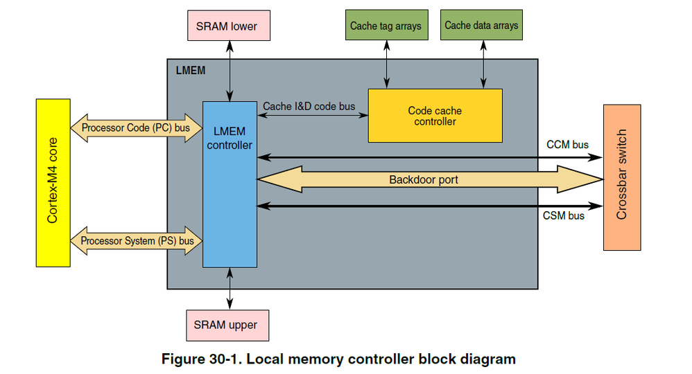
I am sorry for confusion. The Code Cache can be enabled for the DRAM controller on the K65 derivative according to the reference manual. This cache can be used for access the SDRAM memory by the Program Code (I&D code) bus but the System Bus does not use any cache, see the following block diagram of K65 derivatives.
The K65 Reference Manual contains also following information:
30.4.1.1 Processor Code accesses
Processor Code accesses are routed to the SRAM_L if they are mapped to that space. All other PC accesses are routed to the Code Cache Memory Controller. This controller then processes the cacheable accesses as needed, while bypassing the non-cacheable, cache write-through, cache miss, and cache maintenance accesses to the CCM bus and the crossbar switch using the Master0 port.
30.4.1.2 Processor System accesses
Processor Space accesses are routed to the SRAM_U if they are mapped to that space. All other PS accesses are routed to the CCM bus and the crossbar switch using the Master1 port.
30.4.1.3 Backdoor port accesses
All LMEM backdoor port accesses are for the SRAM controller. These accesses go to the SRAM_L or the SRAM_U depending on their specific address.
The Optimizing Performance on Kinetis K-series MCUs application note contains the following information:
- ICODE - The ICODE bus is used for instruction accesses for any instructions stored between addresses 0x0000_0000-0x1FFF_FFFF.
- DCODE - The DCODE bus is used for data accesses for any instructions store between addresses 0x0000_0000-0x1FFF_FFFF.
- System - The system bus is used for all accesses to addresses between 0x2000_0000-0xDFFF_FFFF and 0xE010_0000-0xFFFF_FFFF
Therefore the only way how to use cache is the using of 0x08000000 - 0x08800000 memory area. But this memory area can be used in the write-through cache mode only (write-back mode is not available).
I will also send a question to an internal specialist about the usage of the cache and definition of cache regions. It is not clear from the description in the K65 reference manual.
Note:
Please, consider also the following information about write-back mode of the cache.
• A write-back write miss will do a "read-to-write" (allocate on write miss policy
for write-back mode spaces). A line read on the output bus of a 16 byte aligned
memory address containing the desired write address is performed. This miss
data is loaded into the cache and marked as valid and modified; and the write
data will then update the appropriate cache data locations.
It is mean, that writing into SDRAM memory performs reading of 16 bytes of memory into the cache and writing back into SDRAM memory. When you execute long sequence of writing into SDRAM it leads to reading and writing of the whole memory block from/to SDRAM.
Best Regards,
Marek Neuzil
- Mark as New
- Bookmark
- Subscribe
- Mute
- Subscribe to RSS Feed
- Permalink
- Report Inappropriate Content
to conclude your answer and express what i have understood:
there is no caching of DATA possible, but CODE from external SDRAM?
- Mark as New
- Bookmark
- Subscribe
- Mute
- Subscribe to RSS Feed
- Permalink
- Report Inappropriate Content
Hi Peter,
You are right, the only CODE from SDRAM can be cached (Region 1). The K65 core CPU can use the following regions only (R5-R15 regions are not available because the System Cache is not available on K65).
(I have received a confirmation of this fact from a Freescale specialist)
Note:
The SDRAM controller contains 16-bytes buffer. It should be able to buffer at least 16-bytes of data (line transfer size).
Best Regards,
Marek Neuzil
- Mark as New
- Bookmark
- Subscribe
- Mute
- Subscribe to RSS Feed
- Permalink
- Report Inappropriate Content
would caching of data on the external SDRAM possible when using a K70 device ?
- Mark as New
- Bookmark
- Subscribe
- Mute
- Subscribe to RSS Feed
- Permalink
- Report Inappropriate Content
Hi Peter,
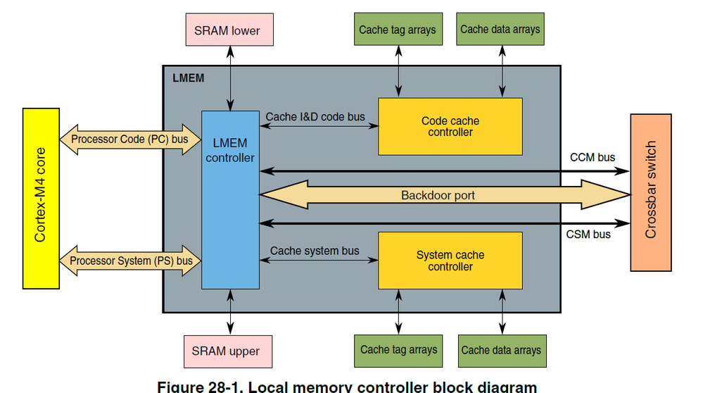
The K70 derivatives contains both caches (for code bus and system bus of the Core), see the following block diagram (K70 subfamily reference manual):
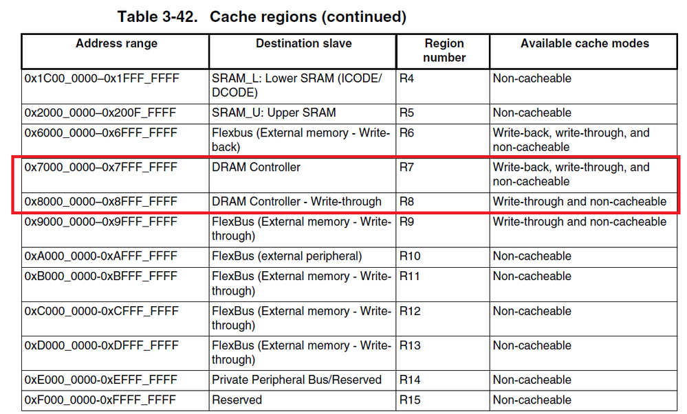
You can use R7 and R8 cache regions to configure cache access to the SDRAM (from the Core):
Note:
R7 region cache mode is is write-back by default (after reset state)
R8 region cache mode is is write-through by default (after reset state)
See details in the Chapter 28 Local Memory Controller in the reference manual of the K70 subfamily.
Best Regards,
Marek Neuzil
- Mark as New
- Bookmark
- Subscribe
- Mute
- Subscribe to RSS Feed
- Permalink
- Report Inappropriate Content
thank you Markek,
i'm aware that the K70 family contains more extensive cache capabilities.
but does it also cache DATA ?? thats the question I asked in advance of your reply.
- Mark as New
- Bookmark
- Subscribe
- Mute
- Subscribe to RSS Feed
- Permalink
- Report Inappropriate Content
Peter,
The system bus is used for all accesses to addresses between 0x2000_0000-0xDFFF_FFFF and 0xE010_0000-0xFFFF_FFFF by the Core. Therefore the system cache can be used for caching of SDRAM data that are accessed by using 0x7000_0000–0x7FFF_FFFF or 0x8000_0000–0x8FFF_FFFF addresses (R7 and R8 cache regions).
Best Regards,
Marek Neuzil
- Mark as New
- Bookmark
- Subscribe
- Mute
- Subscribe to RSS Feed
- Permalink
- Report Inappropriate Content
Hi Marek,
thanks again for destilling it to a level I can understand :smileyhappy:!
Unfortunately, we can't choose the K70 parts because of its lower flash and SRAM capacity compared to the K65 :smileysad:
very sad that theres no system bus cache on the K65...
Best regards
Peter
- Mark as New
- Bookmark
- Subscribe
- Mute
- Subscribe to RSS Feed
- Permalink
- Report Inappropriate Content
Hey Peter,
What about using the K80? It has big SRAM capacities and a system-bus-cache. Unfortunately the integrated FLASH is quite limited.
Regards
- Mark as New
- Bookmark
- Subscribe
- Mute
- Subscribe to RSS Feed
- Permalink
- Report Inappropriate Content
Hallo Markus,
products in pre-production state are not of any interest for us. there's no way our application can fit in 256K flash either.
External storage in NOR flash is not an option as of security concerns.
regards


