- Forums
- Product Forums
- General Purpose MicrocontrollersGeneral Purpose Microcontrollers
- i.MX Forumsi.MX Forums
- QorIQ Processing PlatformsQorIQ Processing Platforms
- Identification and SecurityIdentification and Security
- Power ManagementPower Management
- Wireless ConnectivityWireless Connectivity
- RFID / NFCRFID / NFC
- Advanced AnalogAdvanced Analog
- MCX Microcontrollers
- S32G
- S32K
- S32V
- MPC5xxx
- Other NXP Products
- S12 / MagniV Microcontrollers
- Powertrain and Electrification Analog Drivers
- Sensors
- Vybrid Processors
- Digital Signal Controllers
- 8-bit Microcontrollers
- ColdFire/68K Microcontrollers and Processors
- PowerQUICC Processors
- OSBDM and TBDML
- S32M
- S32Z/E
-
- Solution Forums
- Software Forums
- MCUXpresso Software and ToolsMCUXpresso Software and Tools
- CodeWarriorCodeWarrior
- MQX Software SolutionsMQX Software Solutions
- Model-Based Design Toolbox (MBDT)Model-Based Design Toolbox (MBDT)
- FreeMASTER
- eIQ Machine Learning Software
- Embedded Software and Tools Clinic
- S32 SDK
- S32 Design Studio
- GUI Guider
- Zephyr Project
- Voice Technology
- Application Software Packs
- Secure Provisioning SDK (SPSDK)
- Processor Expert Software
- Generative AI & LLMs
-
- Topics
- Mobile Robotics - Drones and RoversMobile Robotics - Drones and Rovers
- NXP Training ContentNXP Training Content
- University ProgramsUniversity Programs
- Rapid IoT
- NXP Designs
- SafeAssure-Community
- OSS Security & Maintenance
- Using Our Community
-
- Cloud Lab Forums
-
- Knowledge Bases
- ARM Microcontrollers
- i.MX Processors
- Identification and Security
- Model-Based Design Toolbox (MBDT)
- QorIQ Processing Platforms
- S32 Automotive Processing Platform
- Wireless Connectivity
- CodeWarrior
- MCUXpresso Suite of Software and Tools
- MQX Software Solutions
- RFID / NFC
- Advanced Analog
-
- NXP Tech Blogs
- Home
- :
- General Purpose Microcontrollers
- :
- Kinetis Microcontrollers
- :
- Re: Noise using ADC.
Noise using ADC.
- Subscribe to RSS Feed
- Mark Topic as New
- Mark Topic as Read
- Float this Topic for Current User
- Bookmark
- Subscribe
- Mute
- Printer Friendly Page
- Mark as New
- Bookmark
- Subscribe
- Mute
- Subscribe to RSS Feed
- Permalink
- Report Inappropriate Content
Hello all,
I am working with a FRDM-KL25Z board, and I am having problems with the noise when the ADC starts working.
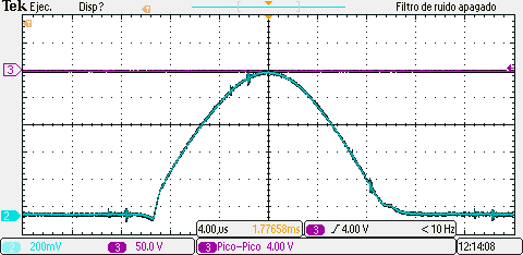
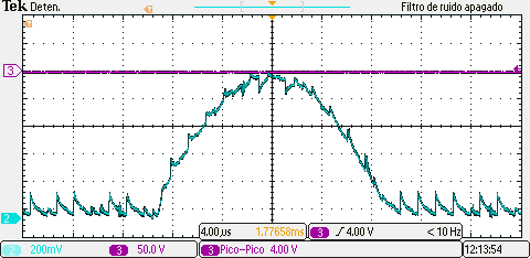
I am analizing a 25KHz signal that is amplified and then is measured by the ADC (pin PTB0/ADC0_SE8). I make several measurements as fast as possible in order to detect the maximum of the signal.
Please find below a picture of the signal in the PTB0 pin when no ADC conversions are taken.
And now, please find below the same signal in the same pin when ADC conversions are being performed.
I placed 1nF capacitor in the PTB0 pin but the the noise is still there.
Could anybody help?
Thank you very much in advance.
Solved! Go to Solution.
- Mark as New
- Bookmark
- Subscribe
- Mute
- Subscribe to RSS Feed
- Permalink
- Report Inappropriate Content
Hi,
Please have a look at AN4373, which shows during the ADC acquisition time, the ADC pin will be charged the sample and hold (S/H) circuit.
It need to make sure the external RC components for SAR ADC conversion result.
Wish it helps.
best regards,
Ma Hui
- Mark as New
- Bookmark
- Subscribe
- Mute
- Subscribe to RSS Feed
- Permalink
- Report Inappropriate Content
Hello Hui_Ma,
I am sorry for not replying you before.
I found the application note very very interesting, and I will try to apply it to my circuit.
The application note help me to understand many concepts of the SAR ADC. Now I see the relation between the short/long sample time and the impedance input.
In our proyect, I need continuous and fast conversions so I need a lower impedance input in order make the capacitors being charged before the conversion is isolated from the input channel. Regarding the sampling time, I have the following doubt about the hight speed conversion:
The KL25 sub-family reference manual says in page 488 that the high speed conversion must be used when the ADCLK exceeds the limit for high ADHSC = 0
What limit is he talking about?
Thank you again.
BR.
- Mark as New
- Bookmark
- Subscribe
- Mute
- Subscribe to RSS Feed
- Permalink
- Report Inappropriate Content
Hi
Unfortunately, there without document shows the ADC high-speed conversion condition.
I had consulted with Kinetis product team, the ADC high-speed conversion means the ADC clock > 8MHz.
Please set the ADCx_CFG2[ADHSC] bit when the ADC clock > 8MHz.
Wish it helps
Have a great day,
Ma Hui
-----------------------------------------------------------------------------------------------------------------------
Note: If this post answers your question, please click the Correct Answer button. Thank you!
-----------------------------------------------------------------------------------------------------------------------
- Mark as New
- Bookmark
- Subscribe
- Mute
- Subscribe to RSS Feed
- Permalink
- Report Inappropriate Content
Hello again Ma Hui.
I keep trying on this and I found a rather strange issue.
Now that I know where the voltage drops come from, I see more drops than there should be. Please let me to explain myself:
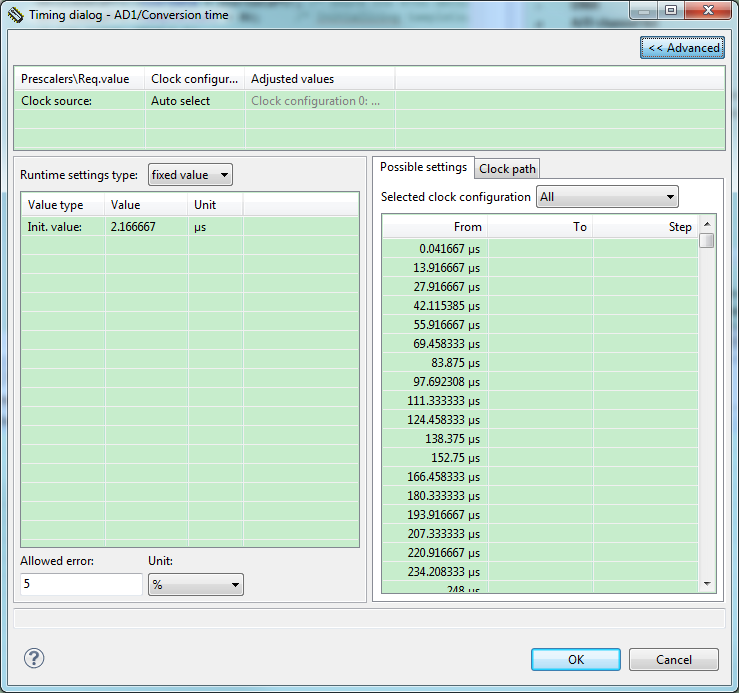
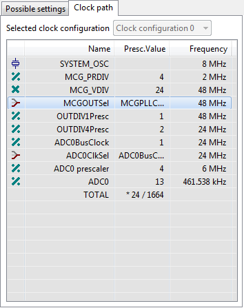
In the following picture you will find my setting for the ADC component. As you can see, the conversion time results in 2.166us.
Some highlights:
- Bus clock = 24MHz.
- ADC clock = 12MHz.
- Number of conversions = 1, which means that no averaging is enabled.
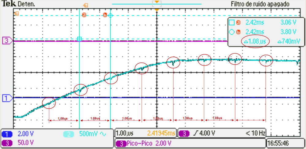
In the picture below the input signal is shown. As I am working in the continuos mode, the signal is converted non stop. The cursors show 1.08us between voltage drops which means every time the sampling capacitor starts changing. It should happen every 2.16us but the osciloscope shows that is every 1.08us (suspiciously half of 2.16us)
In order to see what is going on, I decided to complement a pin every ADC conversion completed interrupt (AD1_OnMeasurementComplete).
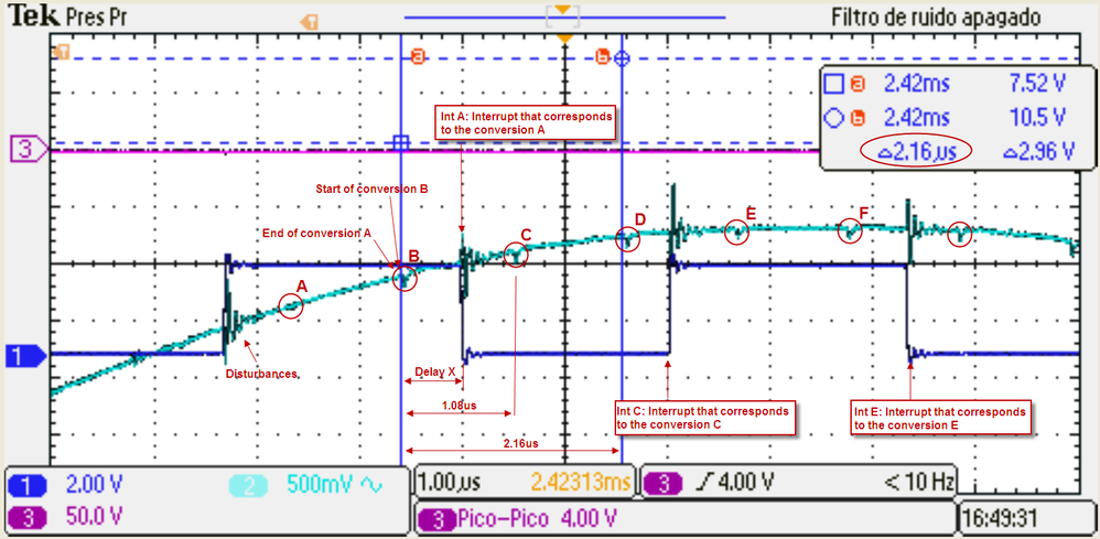
- In the following picture the voltage drops are noted from A to F (every 1.08us).
- The square signal in dark blue shows every time a conversion is completed, and it happen to be every 2.16us !!!!!! (as PE shows)
- Delay X is assumed to be time between the end of the conversion and the complement instruction in the interrupt subroutine.
- When the conversion that corresponds to the drop A finishes, the interrupt is executed and the pin is complemented. Automatically begisns the conversion B.
- When the conversion B finishes, theres is no interrupt and the conversion C starts. It seems that the interrupts from B, D and F are missed.
Note: The disturbances are due to the pin complementing.
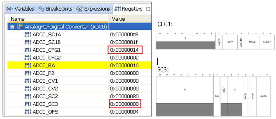
Having seen so strange behaviour, I decided to debug the code in order to read the ADC registers, and this was the result.
SC3 = 0X08, means:
- AVGE = 0 --> Hardware average function disabled.
CFG1 = 0x14, means that:
- ADIV (clock divde select) = 00. --> No prescaler.
- ADICLK (input clock select) = 00. --> Bus clock. ????????? :smileyconfused:
In the first picture, in the PE settings, we saw that Bus clock = 24MHz and ADC clock = 12MHz. The value of CFG1 shows that ADC is working at 24MHz and should be 12MHZ. Is there a divider missing somewhere?
However from the oscilloscope I draw the conclusion that the ADC Clock is working at 24MHz (that would be the reason of the 1.08us instead of 2.16us) and the hardware average function is enabled to make 2 samples average. Nevertheless the AVGE =0 and 4 samples average is the lowest option and not 2 samples average.
Could it be a Processor Expert bug?
Am I missing something in the conversion?
Am I missreading something about voltage drops and convesions?
I hope I explained myself properly.
Thank you in advance.
- Mark as New
- Bookmark
- Subscribe
- Mute
- Subscribe to RSS Feed
- Permalink
- Report Inappropriate Content
Hi
Thank you for the patience.
I found the Processor Expert ADC_LDD component doesn't provide conversion time of 2.1667us option at [Timing Dialog - AD1/Conversion Time] Panel.
I also generated AD1_Init() function, which set ADC clock to 6MHz:
I also get below ADC0_CFG1 register setting, the ADC clock was set to 6MHz:
/* ADC0_CFG1: ??=0,??=0,??=0,??=0,??=0,??=0,??=0,??=0,??=0,??=0,??=0,??=0,??=0,??=0,??=0,??=0,??=0,??=0,??=0,??=0,??=0,??=0,??=0,??=0,ADLPC=0,ADIV=2,ADLSMP=1,MODE=1,ADICLK=0 */
ADC0_CFG1 = ADC_CFG1_ADIV(0x02) |
ADC_CFG1_ADLSMP_MASK |
ADC_CFG1_MODE(0x01) |
ADC_CFG1_ADICLK(0x00);
I need to check with Processor Expert related engineer if the conversion timing setting out of the option could generate the incorrect register setting.
I will be back when there with any feedback.
Have a great day,
Ma Hui
-----------------------------------------------------------------------------------------------------------------------
Note: If this post answers your question, please click the Correct Answer button. Thank you!
-----------------------------------------------------------------------------------------------------------------------
- Mark as New
- Bookmark
- Subscribe
- Mute
- Subscribe to RSS Feed
- Permalink
- Report Inappropriate Content
Hi,
In case it could help, I simply let you know that I am working with CodeWarrior v10.5.
Please make me know if you need any other information.
Thank you.
BR.
Aitor.
- Mark as New
- Bookmark
- Subscribe
- Mute
- Subscribe to RSS Feed
- Permalink
- Report Inappropriate Content
Hello,
I have also checked the ADC_LDD issue in CW MCU 10.6.4 (and also in a previous version) but I am not able to reproduce the issue of the ADC0_CFG1[ADIV] bitfield (prescaler) in the initialization code of the ADC_LDD. Could you provide your application for analysis, please?
Best Regards,
Marek Neuzil
- Mark as New
- Bookmark
- Subscribe
- Mute
- Subscribe to RSS Feed
- Permalink
- Report Inappropriate Content
Ok, thank you again Ma Hui.
