- Forums
- Product Forums
- General Purpose MicrocontrollersGeneral Purpose Microcontrollers
- i.MX Forumsi.MX Forums
- QorIQ Processing PlatformsQorIQ Processing Platforms
- Identification and SecurityIdentification and Security
- Power ManagementPower Management
- Wireless ConnectivityWireless Connectivity
- RFID / NFCRFID / NFC
- Advanced AnalogAdvanced Analog
- MCX Microcontrollers
- S32G
- S32K
- S32V
- MPC5xxx
- Other NXP Products
- S12 / MagniV Microcontrollers
- Powertrain and Electrification Analog Drivers
- Sensors
- Vybrid Processors
- Digital Signal Controllers
- 8-bit Microcontrollers
- ColdFire/68K Microcontrollers and Processors
- PowerQUICC Processors
- OSBDM and TBDML
- S32M
- S32Z/E
-
- Solution Forums
- Software Forums
- MCUXpresso Software and ToolsMCUXpresso Software and Tools
- CodeWarriorCodeWarrior
- MQX Software SolutionsMQX Software Solutions
- Model-Based Design Toolbox (MBDT)Model-Based Design Toolbox (MBDT)
- FreeMASTER
- eIQ Machine Learning Software
- Embedded Software and Tools Clinic
- S32 SDK
- S32 Design Studio
- GUI Guider
- Zephyr Project
- Voice Technology
- Application Software Packs
- Secure Provisioning SDK (SPSDK)
- Processor Expert Software
- Generative AI & LLMs
-
- Topics
- Mobile Robotics - Drones and RoversMobile Robotics - Drones and Rovers
- NXP Training ContentNXP Training Content
- University ProgramsUniversity Programs
- Rapid IoT
- NXP Designs
- SafeAssure-Community
- OSS Security & Maintenance
- Using Our Community
-
- Cloud Lab Forums
-
- Knowledge Bases
- ARM Microcontrollers
- i.MX Processors
- Identification and Security
- Model-Based Design Toolbox (MBDT)
- QorIQ Processing Platforms
- S32 Automotive Processing Platform
- Wireless Connectivity
- CodeWarrior
- MCUXpresso Suite of Software and Tools
- MQX Software Solutions
- RFID / NFC
- Advanced Analog
-
- NXP Tech Blogs
- Home
- :
- General Purpose Microcontrollers
- :
- Kinetis Microcontrollers
- :
- Re: KL02 Input voltage operating requirements
KL02 Input voltage operating requirements
- Subscribe to RSS Feed
- Mark Topic as New
- Mark Topic as Read
- Float this Topic for Current User
- Bookmark
- Subscribe
- Mute
- Printer Friendly Page
- Mark as New
- Bookmark
- Subscribe
- Mute
- Subscribe to RSS Feed
- Permalink
- Report Inappropriate Content
Please help to confirm the below questions,
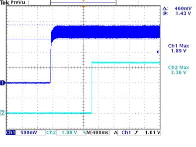
- 1) The below waveform is our test waveform, and the test condition is:
- Ch1 is input signal to pin11, and Ch2 is output signal from pin22
- Pin11 and pin22 are configured GPIO
- The logic level of Ch2 is the same with Ch1. For example, if Ch1 goes high, then Ch2 goes high too.
From the datasheet, the input high voltage of KL02 device is about 3.3V * 0.7 = 2.31V.
But, according to our experiment, the output signal goes high even the input signal is about 1.43V ~ 1.89V. Please help to check the input high/low voltage level.
The CH1 max voltage is 1.89V, min voltage is 1.43V, it's available without this voltage range.
Please help to confirm input high/low voltage level first, thanks.
Solved! Go to Solution.
- Mark as New
- Bookmark
- Subscribe
- Mute
- Subscribe to RSS Feed
- Permalink
- Report Inappropriate Content
Hello Kris,
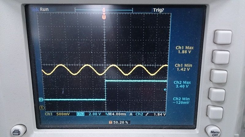
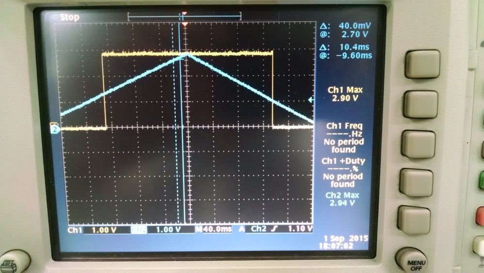
I recreated the scenario and as you can see in the image shown below, I found very similar results
The rising edge will toggle the pin's input buffer at about 0.7 * VDD Volts while the falling edge will toggle the input buffer at about 0.35 * VDD Volts. These are the actual input buffer transition points, also known as threshold voltages. The VIL and VIH calculations are to guarantee logic levels – the switch points are well within the VIL/VIH specs. The input buffer thresholds change with VDD, temp, and process, so we cannot guarantee the switchpoint voltages, however, they are within the VIL/VIH limits. And, the difference between the switchpoints will be at least as much as the hysteresis spec, which is about 200mV at VDD = 3.3V.
Please let me know if this information is useful or if I can do anything else for you.
Best regards,
Earl Orlando.
/* If this post answers your question please click the Correct Answer button. */
- Mark as New
- Bookmark
- Subscribe
- Mute
- Subscribe to RSS Feed
- Permalink
- Report Inappropriate Content
Hi Earl
Thanks your feedback.
As I know, From theory, the I/O cell is an CMOS circuit, Does the a middle voltage will turn on both MOS gate which will leads to damage?
Is there any suggestions to address this issue?
What if we have an logic I/O to the KL02, but the slew rate of the signal is a bit slow, will there be an issue for the VIH/VIL?
If so, what is the acceptable slew rate for the I/O ports in your device.
- Mark as New
- Bookmark
- Subscribe
- Mute
- Subscribe to RSS Feed
- Permalink
- Report Inappropriate Content
Hello Kris,
I am sorry for the delay on my part. The middle voltage range does not damage the I/O cell. The only one issue that you could experiment is the change of the thresholds to toggle from low to high and vice-versa.
Best regards,
Earl.


