- Forums
- Product Forums
- General Purpose MicrocontrollersGeneral Purpose Microcontrollers
- i.MX Forumsi.MX Forums
- QorIQ Processing PlatformsQorIQ Processing Platforms
- Identification and SecurityIdentification and Security
- Power ManagementPower Management
- Wireless ConnectivityWireless Connectivity
- RFID / NFCRFID / NFC
- Advanced AnalogAdvanced Analog
- MCX Microcontrollers
- S32G
- S32K
- S32V
- MPC5xxx
- Other NXP Products
- S12 / MagniV Microcontrollers
- Powertrain and Electrification Analog Drivers
- Sensors
- Vybrid Processors
- Digital Signal Controllers
- 8-bit Microcontrollers
- ColdFire/68K Microcontrollers and Processors
- PowerQUICC Processors
- OSBDM and TBDML
- S32M
- S32Z/E
-
- Solution Forums
- Software Forums
- MCUXpresso Software and ToolsMCUXpresso Software and Tools
- CodeWarriorCodeWarrior
- MQX Software SolutionsMQX Software Solutions
- Model-Based Design Toolbox (MBDT)Model-Based Design Toolbox (MBDT)
- FreeMASTER
- eIQ Machine Learning Software
- Embedded Software and Tools Clinic
- S32 SDK
- S32 Design Studio
- GUI Guider
- Zephyr Project
- Voice Technology
- Application Software Packs
- Secure Provisioning SDK (SPSDK)
- Processor Expert Software
- Generative AI & LLMs
-
- Topics
- Mobile Robotics - Drones and RoversMobile Robotics - Drones and Rovers
- NXP Training ContentNXP Training Content
- University ProgramsUniversity Programs
- Rapid IoT
- NXP Designs
- SafeAssure-Community
- OSS Security & Maintenance
- Using Our Community
-
- Cloud Lab Forums
-
- Knowledge Bases
- ARM Microcontrollers
- i.MX Processors
- Identification and Security
- Model-Based Design Toolbox (MBDT)
- QorIQ Processing Platforms
- S32 Automotive Processing Platform
- Wireless Connectivity
- CodeWarrior
- MCUXpresso Suite of Software and Tools
- MQX Software Solutions
- RFID / NFC
- Advanced Analog
-
- NXP Tech Blogs
- Home
- :
- 汎用マイクロコントローラ
- :
- Kinetisマイクロコントローラ
- :
- FRDM K64F FTM + DMA for SPWM Generation
FRDM K64F FTM + DMA for SPWM Generation
- RSS フィードを購読する
- トピックを新着としてマーク
- トピックを既読としてマーク
- このトピックを現在のユーザーにフロートします
- ブックマーク
- 購読
- ミュート
- 印刷用ページ
- 新着としてマーク
- ブックマーク
- 購読
- ミュート
- RSS フィードを購読する
- ハイライト
- 印刷
- 不適切なコンテンツを報告
Hello,
I'm working on an SPWM (sine wave pulse width modulation) setup in which a block of memory is written via DMA to the CnV register of a FTM (FlexTimer Module).
I have a setup in which no DMA is used and the FTM duty cycle is updated in the main loop (very dirty). This arrangement works fine but consumes a lot of CPU cycles that I would rather use for other things. The FTM CnV buffer is written to the register when the API (https://mcuxpresso.nxp.com/api_doc/dev/974/group__ftm.html#ga08e1b1c36631d42a77a5e08d76884d8b) function
FTM_SetSoftwareTrigger(FTM_0_PERIPHERAL, true);
is called.
The DMA setup shows no error flags in the DMA error status register, so I'm reasonably confident that it is set up ok. However, when I connect the DMAMUX to FTM CnV channel and try to run the FTM with CnV updates via DMA the FTM duty cycle is fixed at its initialisation value.
I suspect there is an option register in the FTM that I'm not setting which tells the FTM to ask the DMA for the next CnV value and update the CnV register from the buffer when the FTM counter rolls over. I am aware of the DMA bit in the FTM CnSC register but I think there must be a hardware trigger bit that I need to either enable or have the DMA fire when it updates the buffer.
Any assistance would be much appreciated.
解決済! 解決策の投稿を見る。
- 新着としてマーク
- ブックマーク
- 購読
- ミュート
- RSS フィードを購読する
- ハイライト
- 印刷
- 不適切なコンテンツを報告
James
To be sure that you can accept a solution I have copied below the bare metal version of the function. It has three versions:
1. A basic bare metal one using high efficiency macros and defines that should be understandable but you would need to replace them with your own version,
2. A very bare metal version which doesn't use macros or defines for the register values - this may be usable if you have register address defines.
3. A super bare metal one that uses no macros or defines (apart from the register blocks) that will run in any environment.
I tested each one on the FRDM-K64F so you will just need to set up the channels that you want to use. The code should help you identify what is missing in your version in case you don't want to use this one.
The routines is passed a pointer to the SPWM table and its physical length and then it runs free-run and will also continue when the debugger freezes the CPU..
static void fnBareMetalSPWM(unsigned short *ptrBuffer, unsigned long ulBufferLength)
{
POWER_UP_ATOMIC(6, FTM0); // ensure that the FlexTimer/TPM module is powered up
_CONFIG_PERIPHERAL(C, 3, (PC_3_FTM0_CH2 | (PORT_SRE_FAST | PORT_DSE_HIGH))); // FTM0_CH2 on PC.3 (alt. function 4)
FTM0_CONF = FTM_CONF_BDMMODE_3; // allow timer to continue operating when debugging
FTM0_C2SC = (FTM_CSC_MS_ELS_PWM_HIGH_TRUE_PULSES | FTM_CSC_DMA | FTM_CSC_CHIE); // high-true pulses/enable DMA trigger from this channel
FTM0_CNTIN = 0;
FTM0_MOD = 0xffff;
FTM0_C2V = *ptrBuffer; // prepare first PWM value
DMA_TCD1_SOFF = sizeof(unsigned short); // source increment (buffer)
DMA_TCD1_DOFF = 0; // destination not incremented
DMA_TCD1_DLASTSGA = 0; // no destination displacement on transmit buffer completion
DMA_TCD1_SLAST = (-(signed long)(ulBufferLength));// when the buffer has been transmitted set the destination back to the start of it
DMA_TCD1_ATTR = (DMA_TCD_ATTR_DSIZE_16 | DMA_TCD_ATTR_SSIZE_16); // transfer sizes half-words
DMA_TCD1_SADDR = (unsigned long)ptrBuffer; // source buffer
DMA_TCD1_CSR = 0; // free-running mode without any interrupt
DMA_TCD1_DADDR = (unsigned long)FTM0_C2V_ADDRESS; // // destination address is the PWM register
DMA_TCD1_NBYTES_MLNO = sizeof(unsigned short); // each request starts a single transfer of this size (minor byte transfer count)
DMA_TCD1_BITER_ELINKNO = DMA_TCD1_CITER_ELINKNO = (signed short)(ulBufferLength / sizeof(unsigned short)); // the number of service requests to be performed each buffer cycle
POWER_UP_ATOMIC(6, DMAMUX0); // enable DMA multiplexer 0
DMAMUX0_CHCFG1 = (DMA_MUX_REGISTER)(DMAMUX0_CHCFG_SOURCE_FTM0_C2 | DMAMUX_CHCFG_ENBL); // connect trigger source to DMA channel
ATOMIC_PERIPHERAL_BIT_REF_SET(DMA_ERQ, 1); // enable the channel's operation
FTM0_SC = PWM_SYS_CLK; // enable FTM0 operation (system clock)
}
static void fnBareMetalSPWM(unsigned short *ptrBuffer, unsigned long ulBufferLength)
{
SIM_SCGC6 |= 0x01000000; // ensure that the FlexTimer/TPM module is powered up
SIM_SCGC5 |= 0x00000800;
PORTC_PCR3 = (0x00000400 | 0x00000040); // FTM0_CH2 on PC.3 (alt. function 4)
FTM0_CONF = 0x000000c0; // allow timer to continue operating when debugging
FTM0_C2SC = (0x00000020 | 0x00000008 | 0x00000001 | 0x00000040); // high-true pulses/enable DMA trigger from this channel
FTM0_CNTIN = 0;
FTM0_MOD = 0xffff;
FTM0_C2V = *ptrBuffer; // prepare first PWM value
DMA_TCD1_SOFF = sizeof(unsigned short); // source increment (buffer)
DMA_TCD1_DOFF = 0; // destination not incremented
DMA_TCD1_DLASTSGA = 0; // no destination displacement on transmit buffer completion
DMA_TCD1_SLAST = (-(signed long)(ulBufferLength));// when the buffer has been transmitted set the destination back to the start of it
DMA_TCD1_ATTR = (0x0001 | 0x0100); // transfer sizes half-words
DMA_TCD1_SADDR = (unsigned long)ptrBuffer; // source buffer
DMA_TCD1_CSR = 0; // free-running mode without any interrupt
DMA_TCD1_DADDR = (unsigned long)((0x40038000 + 0x020)); // destination address is the PWM register
DMA_TCD1_NBYTES_MLNO = sizeof(unsigned short); // each request starts a single transfer of this size (minor byte transfer count)
DMA_TCD1_BITER_ELINKNO = DMA_TCD1_CITER_ELINKNO = (signed short)(ulBufferLength / sizeof(unsigned short)); // the number of service requests to be performed each buffer cycle
SIM_SCGC6 |= 0x00000002; // enable DMA multiplexer 0
DMAMUX0_CHCFG1 = (unsigned char)(0x16 | 0x80); // connect trigger source to DMA channel
DMA_ERQ |= 0x00000002; // enable the channel's operation
FTM0_SC = 0x00000008; // enable FTM0 operation (system clock)
}
static void fnBareMetalSPWM(unsigned short *ptrBuffer, unsigned long ulBufferLength)
{
#define SIM_BLOCK 0x40047000 // system integration module
#define PORT2_BLOCK 0x4004b000
#define FTM_BLOCK_0 0x40038000 // FlexTimer 0 (TPM0)
#define eDMA_DESCRIPTORS 0x40009000 // eDMA Descriptor Memory
#define DMAMUX0_BLOCK 0x40021000 // DMAMUX0
*(volatile unsigned long *)(SIM_BLOCK + 0x103c) |= 0x01000000; // ensure that the FlexTimer/TPM module is powered up
*(volatile unsigned long*)(SIM_BLOCK + 0x1038) |= 0x00000800;
*(volatile unsigned long *)(PORT2_BLOCK + 0x0c) = (0x00000400 | 0x00000040); // FTM0_CH2 on PC.3 (alt. function 4)
*(unsigned long *)(FTM_BLOCK_0 + 0x084) = 0x000000c0; // allow timer to continue operating when debugging
*(volatile unsigned long *)(FTM_BLOCK_0 + 0x01c) = (0x00000020 | 0x00000008 | 0x00000001 | 0x00000040); // high-true pulses/enable DMA trigger from this channel
*(volatile unsigned long *)(FTM_BLOCK_0 + 0x04c) = 0;
*(unsigned long *)(FTM_BLOCK_0 + 0x008) = 0xffff;
*(volatile unsigned long *)(FTM_BLOCK_0 + FTM_OFFSET_1 + 0x020) = *ptrBuffer; // prepare first PWM value
*(signed short *)(eDMA_DESCRIPTORS + 0x024) = sizeof(unsigned short); // source increment (buffer)
*(signed short *)(eDMA_DESCRIPTORS + 0x034) = 0; // destination not incremented
*(volatile signed long *)(eDMA_DESCRIPTORS + 0x038) = 0; // no destination displacement on transmit buffer completion
*(volatile unsigned long *)(eDMA_DESCRIPTORS + 0x02c) = (-(signed long)(ulBufferLength));// when the buffer has been transmitted set the destination back to the start of it
*(unsigned short *)(eDMA_DESCRIPTORS + 0x026) = (0x0001 | 0x0100); // transfer sizes half-words
*(volatile unsigned long *)(eDMA_DESCRIPTORS + 0x020) = (unsigned long)ptrBuffer; // source buffer
*(volatile unsigned short *)(eDMA_DESCRIPTORS + 0x03c) = 0; // free-running mode without any interrupt
*(volatile unsigned long *)(eDMA_DESCRIPTORS + 0x030) = (unsigned long)((0x40038000 + 0x020)); // destination address is the PWM register
*(volatile unsigned long *)(eDMA_DESCRIPTORS + 0x028) = sizeof(unsigned short); // each request starts a single transfer of this size (minor byte transfer count)
*(unsigned short *)(eDMA_DESCRIPTORS + 0x03e) = *(volatile signed short *)(eDMA_DESCRIPTORS + 0x036) = (signed short)(ulBufferLength / sizeof(unsigned short)); // the number of service requests to be performed each buffer cycle
*(volatile unsigned long *)(SIM_BLOCK + 0x103c) |= 0x00000002; // enable DMA multiplexer 0
*(unsigned char *)(DMAMUX0_BLOCK + 0x01) = (unsigned char)(0x16 | 0x80); // connect trigger source to DMA channel
*(volatile unsigned long *)(eDMA_BLOCK + 0x00c) |= 0x00000002; // enable the channel's operation
*(volatile unsigned long *)(FTM_BLOCK_0 + 0x000) = 0x00000008; // enable FTM0 operation (system clock)
}
Example of use:
#define LENGTH_OF_TEST_BUFFER 128
static unsigned short PWMTestBuffer[128];
// fill buffer with the periodic PWM signal to be generated
fnBareMetalSPWM(PWMTestBuffer, sizeof(PWMTestBuffer)); // start operation
.. continue with other stuff
Regards
Mark
- 新着としてマーク
- ブックマーク
- 購読
- ミュート
- RSS フィードを購読する
- ハイライト
- 印刷
- 不適切なコンテンツを報告
Hi James,
Would you please attach your test project?
So that I can check the problem.
Best Regards,
Robin
- 新着としてマーク
- ブックマーク
- 購読
- ミュート
- RSS フィードを購読する
- ハイライト
- 印刷
- 不適切なコンテンツを報告
Hi Robin,
The project contains commercially sensitive code. If you are acting on behalf of NXP and will not publish the code I’d be very happy for your help and in that case I will send the code.
If you will publish the code then I can’t send it. I could send a portion of it but that wouldn’t allow you to do much testing.
Thanks,
James
- 新着としてマーク
- ブックマーク
- 購読
- ミュート
- RSS フィードを購読する
- ハイライト
- 印刷
- 不適切なコンテンツを報告
James
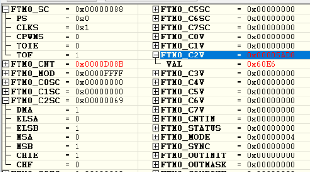
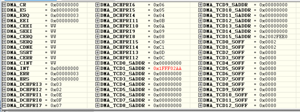
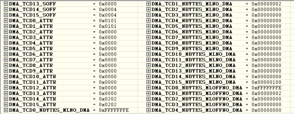
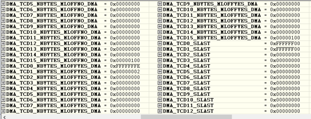
To make to easier for you to reverse engineer the method that I set up for you I have some screen shots of the registers involved:
DMA channel 1 is used and the DMAMUX is connected to the FTM0 channel 2.
These are the FTM registers of interest:
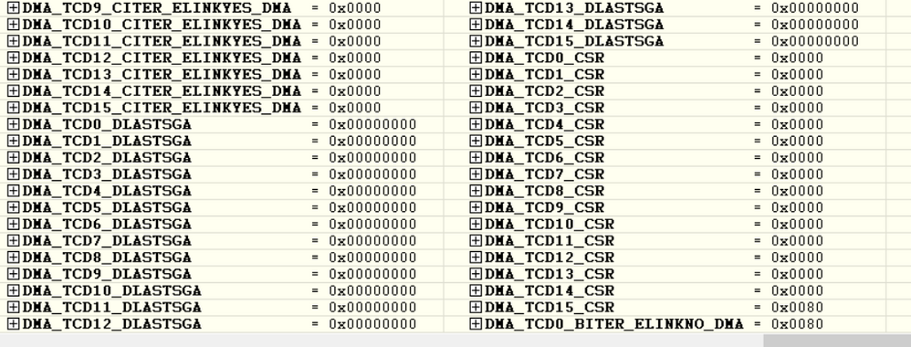
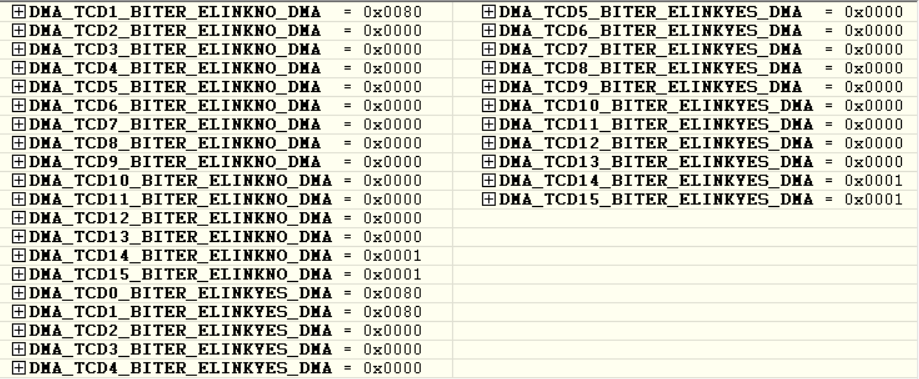
DMA controller registers (snap short when operating) - channel 1 of interest (channels 0 and 15 are also in operation but can be ignored)
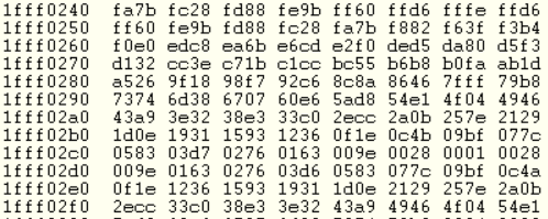
This is the block of memory that the DMA channel 1 source pointer is using, where the SINE PWM pattern can be seen:
If you compare with your setup (and interpolate for the channel and trigger source you are using) you may find a difference that explains the problem. As noted previously a typical mistake is not not set the CHIE flag in the FTM channel register when using DMA because BOTH CHIE and DMA flags need to be enabled for the DMA trigger to operate.
Regards
Mark
Complete Kinetis solutions for professional needs, training and support:http://www.utasker.com/kinetis.html
uTasker: supporting >1'000 registered Kinetis users get products faster and cheaper to market
Request Free emergency remote desk-top consulting at http://www.utasker.com/services.html
- 新着としてマーク
- ブックマーク
- 購読
- ミュート
- RSS フィードを購読する
- ハイライト
- 印刷
- 不適切なコンテンツを報告
Hi Mark,
This is a commercial project and the requirements say it has to be bare metal I’m afraid. Many thanks for your effort though.
Best,
James
- 新着としてマーク
- ブックマーク
- 購読
- ミュート
- RSS フィードを購読する
- ハイライト
- 印刷
- 不適切なコンテンツを報告
James
Use your debugger and pause your (not yet working) code when it "should" be generating the output but is only generating a fixed PWM signal.
Then compare the registers that you see with the ones that I have shown to see what is different/missing - then you can correct your code appropriately (you will probably find just one flag that hasn't been correctly set).
If you have no success, post your binary file that should be generating the signal (no need for any source code) so I can load it to my FRDM-K64F and then tell you why it is not operating as intended.
Regards
Mark
P.S. My code is also bare metal code if the HAL is bypassed so this part could be copied by anyone without violating project specifications.
- 新着としてマーク
- ブックマーク
- 購読
- ミュート
- RSS フィードを購読する
- ハイライト
- 印刷
- 不適切なコンテンツを報告
James
To be sure that you can accept a solution I have copied below the bare metal version of the function. It has three versions:
1. A basic bare metal one using high efficiency macros and defines that should be understandable but you would need to replace them with your own version,
2. A very bare metal version which doesn't use macros or defines for the register values - this may be usable if you have register address defines.
3. A super bare metal one that uses no macros or defines (apart from the register blocks) that will run in any environment.
I tested each one on the FRDM-K64F so you will just need to set up the channels that you want to use. The code should help you identify what is missing in your version in case you don't want to use this one.
The routines is passed a pointer to the SPWM table and its physical length and then it runs free-run and will also continue when the debugger freezes the CPU..
static void fnBareMetalSPWM(unsigned short *ptrBuffer, unsigned long ulBufferLength)
{
POWER_UP_ATOMIC(6, FTM0); // ensure that the FlexTimer/TPM module is powered up
_CONFIG_PERIPHERAL(C, 3, (PC_3_FTM0_CH2 | (PORT_SRE_FAST | PORT_DSE_HIGH))); // FTM0_CH2 on PC.3 (alt. function 4)
FTM0_CONF = FTM_CONF_BDMMODE_3; // allow timer to continue operating when debugging
FTM0_C2SC = (FTM_CSC_MS_ELS_PWM_HIGH_TRUE_PULSES | FTM_CSC_DMA | FTM_CSC_CHIE); // high-true pulses/enable DMA trigger from this channel
FTM0_CNTIN = 0;
FTM0_MOD = 0xffff;
FTM0_C2V = *ptrBuffer; // prepare first PWM value
DMA_TCD1_SOFF = sizeof(unsigned short); // source increment (buffer)
DMA_TCD1_DOFF = 0; // destination not incremented
DMA_TCD1_DLASTSGA = 0; // no destination displacement on transmit buffer completion
DMA_TCD1_SLAST = (-(signed long)(ulBufferLength));// when the buffer has been transmitted set the destination back to the start of it
DMA_TCD1_ATTR = (DMA_TCD_ATTR_DSIZE_16 | DMA_TCD_ATTR_SSIZE_16); // transfer sizes half-words
DMA_TCD1_SADDR = (unsigned long)ptrBuffer; // source buffer
DMA_TCD1_CSR = 0; // free-running mode without any interrupt
DMA_TCD1_DADDR = (unsigned long)FTM0_C2V_ADDRESS; // // destination address is the PWM register
DMA_TCD1_NBYTES_MLNO = sizeof(unsigned short); // each request starts a single transfer of this size (minor byte transfer count)
DMA_TCD1_BITER_ELINKNO = DMA_TCD1_CITER_ELINKNO = (signed short)(ulBufferLength / sizeof(unsigned short)); // the number of service requests to be performed each buffer cycle
POWER_UP_ATOMIC(6, DMAMUX0); // enable DMA multiplexer 0
DMAMUX0_CHCFG1 = (DMA_MUX_REGISTER)(DMAMUX0_CHCFG_SOURCE_FTM0_C2 | DMAMUX_CHCFG_ENBL); // connect trigger source to DMA channel
ATOMIC_PERIPHERAL_BIT_REF_SET(DMA_ERQ, 1); // enable the channel's operation
FTM0_SC = PWM_SYS_CLK; // enable FTM0 operation (system clock)
}
static void fnBareMetalSPWM(unsigned short *ptrBuffer, unsigned long ulBufferLength)
{
SIM_SCGC6 |= 0x01000000; // ensure that the FlexTimer/TPM module is powered up
SIM_SCGC5 |= 0x00000800;
PORTC_PCR3 = (0x00000400 | 0x00000040); // FTM0_CH2 on PC.3 (alt. function 4)
FTM0_CONF = 0x000000c0; // allow timer to continue operating when debugging
FTM0_C2SC = (0x00000020 | 0x00000008 | 0x00000001 | 0x00000040); // high-true pulses/enable DMA trigger from this channel
FTM0_CNTIN = 0;
FTM0_MOD = 0xffff;
FTM0_C2V = *ptrBuffer; // prepare first PWM value
DMA_TCD1_SOFF = sizeof(unsigned short); // source increment (buffer)
DMA_TCD1_DOFF = 0; // destination not incremented
DMA_TCD1_DLASTSGA = 0; // no destination displacement on transmit buffer completion
DMA_TCD1_SLAST = (-(signed long)(ulBufferLength));// when the buffer has been transmitted set the destination back to the start of it
DMA_TCD1_ATTR = (0x0001 | 0x0100); // transfer sizes half-words
DMA_TCD1_SADDR = (unsigned long)ptrBuffer; // source buffer
DMA_TCD1_CSR = 0; // free-running mode without any interrupt
DMA_TCD1_DADDR = (unsigned long)((0x40038000 + 0x020)); // destination address is the PWM register
DMA_TCD1_NBYTES_MLNO = sizeof(unsigned short); // each request starts a single transfer of this size (minor byte transfer count)
DMA_TCD1_BITER_ELINKNO = DMA_TCD1_CITER_ELINKNO = (signed short)(ulBufferLength / sizeof(unsigned short)); // the number of service requests to be performed each buffer cycle
SIM_SCGC6 |= 0x00000002; // enable DMA multiplexer 0
DMAMUX0_CHCFG1 = (unsigned char)(0x16 | 0x80); // connect trigger source to DMA channel
DMA_ERQ |= 0x00000002; // enable the channel's operation
FTM0_SC = 0x00000008; // enable FTM0 operation (system clock)
}
static void fnBareMetalSPWM(unsigned short *ptrBuffer, unsigned long ulBufferLength)
{
#define SIM_BLOCK 0x40047000 // system integration module
#define PORT2_BLOCK 0x4004b000
#define FTM_BLOCK_0 0x40038000 // FlexTimer 0 (TPM0)
#define eDMA_DESCRIPTORS 0x40009000 // eDMA Descriptor Memory
#define DMAMUX0_BLOCK 0x40021000 // DMAMUX0
*(volatile unsigned long *)(SIM_BLOCK + 0x103c) |= 0x01000000; // ensure that the FlexTimer/TPM module is powered up
*(volatile unsigned long*)(SIM_BLOCK + 0x1038) |= 0x00000800;
*(volatile unsigned long *)(PORT2_BLOCK + 0x0c) = (0x00000400 | 0x00000040); // FTM0_CH2 on PC.3 (alt. function 4)
*(unsigned long *)(FTM_BLOCK_0 + 0x084) = 0x000000c0; // allow timer to continue operating when debugging
*(volatile unsigned long *)(FTM_BLOCK_0 + 0x01c) = (0x00000020 | 0x00000008 | 0x00000001 | 0x00000040); // high-true pulses/enable DMA trigger from this channel
*(volatile unsigned long *)(FTM_BLOCK_0 + 0x04c) = 0;
*(unsigned long *)(FTM_BLOCK_0 + 0x008) = 0xffff;
*(volatile unsigned long *)(FTM_BLOCK_0 + FTM_OFFSET_1 + 0x020) = *ptrBuffer; // prepare first PWM value
*(signed short *)(eDMA_DESCRIPTORS + 0x024) = sizeof(unsigned short); // source increment (buffer)
*(signed short *)(eDMA_DESCRIPTORS + 0x034) = 0; // destination not incremented
*(volatile signed long *)(eDMA_DESCRIPTORS + 0x038) = 0; // no destination displacement on transmit buffer completion
*(volatile unsigned long *)(eDMA_DESCRIPTORS + 0x02c) = (-(signed long)(ulBufferLength));// when the buffer has been transmitted set the destination back to the start of it
*(unsigned short *)(eDMA_DESCRIPTORS + 0x026) = (0x0001 | 0x0100); // transfer sizes half-words
*(volatile unsigned long *)(eDMA_DESCRIPTORS + 0x020) = (unsigned long)ptrBuffer; // source buffer
*(volatile unsigned short *)(eDMA_DESCRIPTORS + 0x03c) = 0; // free-running mode without any interrupt
*(volatile unsigned long *)(eDMA_DESCRIPTORS + 0x030) = (unsigned long)((0x40038000 + 0x020)); // destination address is the PWM register
*(volatile unsigned long *)(eDMA_DESCRIPTORS + 0x028) = sizeof(unsigned short); // each request starts a single transfer of this size (minor byte transfer count)
*(unsigned short *)(eDMA_DESCRIPTORS + 0x03e) = *(volatile signed short *)(eDMA_DESCRIPTORS + 0x036) = (signed short)(ulBufferLength / sizeof(unsigned short)); // the number of service requests to be performed each buffer cycle
*(volatile unsigned long *)(SIM_BLOCK + 0x103c) |= 0x00000002; // enable DMA multiplexer 0
*(unsigned char *)(DMAMUX0_BLOCK + 0x01) = (unsigned char)(0x16 | 0x80); // connect trigger source to DMA channel
*(volatile unsigned long *)(eDMA_BLOCK + 0x00c) |= 0x00000002; // enable the channel's operation
*(volatile unsigned long *)(FTM_BLOCK_0 + 0x000) = 0x00000008; // enable FTM0 operation (system clock)
}
Example of use:
#define LENGTH_OF_TEST_BUFFER 128
static unsigned short PWMTestBuffer[128];
// fill buffer with the periodic PWM signal to be generated
fnBareMetalSPWM(PWMTestBuffer, sizeof(PWMTestBuffer)); // start operation
.. continue with other stuff
Regards
Mark
- 新着としてマーク
- ブックマーク
- 購読
- ミュート
- RSS フィードを購読する
- ハイライト
- 印刷
- 不適切なコンテンツを報告
Hi Mark,
Many thanks for your effort. It has been very helpful in encouraging me to abandon the MCUExpresso API and hard code this part of the firmware. I selected your third approach, the most low level because it is the easiest to follow in terms of the register data needed to set everything up and stepping through the code it’s easy to see where one should be looking for changes in the registers when each line has the memory address written in the macro.
There is still a mistake in what’s copied below. It puts out 10kHz (at 120 MHz system clock and no FTM pre-scaling) with 50% duty which equates to the first CnV value in the buffer that the DMA should read. Not sure where the mistake(s) are presently as the end of the working day has crept up on me. If you see anything odd please do point it out. I’ll be back at this on Monday. I suspect that the DMA is either not set up quite right (I’m pointing it at the wrong place etc.) or perhaps the FTM is not requesting the next two bytes from the DMA when CNT == MOD. The processor reference guide gives very little detail about how the timer makes the request to the DMA – certainly the request source is set up in the DMAMUX etc. but the FTM diagram on pp 979 of the processor manual doesn’t have a DMA line anywhere (as far as I can see). Similarly Application Note AN5261 only mentions the DMA in the first paragraph and application note AN4560 doesn’t mention the DMA at all.
#define BUFF_LENGTH 16U
#define SIM_BLOCK 0x40047000 // system integration module
#define SIM_PORT_CLK_GATE_OFFSET 0x00001038 // Register that enables the clock gate to the ports.
#define PORTA_BLOCK 0x40049000 // Port A base address.
#define PORTC_BLOCK 0x4004b000 // Port C base address.
#define DMAMUX0_BLOCK 0x40021000 // DMAMUX0
#define FTM0_BASE_ADDR 0x40038000 // FlexTimer 0 (TPM0) base address.
#define FTM0_MOD 0x00000008 // FlexTimer 0 MOD register offset
#define FTM0_C6SC_OFFSET 0x0000003C // Offset for FTM0_C6SC register offset
#define FTM0_C6V_OFFSET 0x00000040 // Offset for FTM0_C6V register offset
#define FTM0_C7SC_OFFSET 0x00000044 // Offset for FTM0_C7SC register offset
#define FTM0_C7V_OFFSET 0x00000048 // Offset for FTM0_C7V register offset
#define FTM0_C0SC_OFFSET 0x0000000C // Offset for FTM0_C0SC register offset
#define FTM0_C0V_OFFSET 0x00000010 // Offset for FTM0_C0V register offset
#define FTM0_C1SC_OFFSET 0x00000014 // Offset for FTM0_C1SC register offset
#define FTM0_C1V_OFFSET 0x00000018 // Offset for FTM0_C1V register offset
#define eDMA_DESCRIPTORS 0x40009000 // eDMA descriptor memory
#define eDMA_BASE_ADDR 0x40008000 // eDMA base Address
static void fnBareMetalSPWM(unsigned short *ptrBuffer, unsigned long ulBufferLength)
{
// System Clock Gating Control Register 5 (SIM_SCGC5), switch on clock for port A
//*(volatile unsigned long *)(SIM_BLOCK + SIM_PORT_CLK_GATE_OFFSET) |= 0x00000200;
// System Clock Gating Control Register 5 (SIM_SCGC5), switch on clock for port C
*(volatile unsigned long *)(SIM_BLOCK + SIM_PORT_CLK_GATE_OFFSET) |= 0x00000800;
// FTM. Ensure that the FlexTimer/TPM module is powered up
*(volatile unsigned long *)(SIM_BLOCK + 0x103c) |= 0x01000000;
// FTM0_CH1 on PTC2 (alt. function 4) and high drive strength
*(volatile unsigned long *)(PORTC_BLOCK + 0x08) = (0x00000400 | 0x00000040);;
// FTM0_CH6 on PTA1 (alt. function 3) and high drive strength
//*(volatile unsigned long *)(PORTA_BLOCK + 0x04) = 0x00000340;
// FTM0_CH7 on PTA2 (alt. function 3)
// *(volatile unsigned long *)(PORTA_BLOCK + 0x08) = (0x00000300 | 0x00000040);
// allow timer to continue operating when debugging
*(unsigned long *)(FTM0_BASE_ADDR + 0x084) = 0x000000c0;
// high-true pulses/enable DMA trigger from this channel
*(volatile unsigned long *)(FTM0_BASE_ADDR + FTM0_C1SC_OFFSET) = (0x00000020 | 0x00000008 | 0x00000001 | 0x00000040);
// Set counter initial value to zero
*(volatile unsigned long *)(FTM0_BASE_ADDR + 0x04c) = 0;
// Set counter MOD register to the value that provides the frequency of interest.
*(unsigned long *)(FTM0_BASE_ADDR + FTM0_MOD) = 0x1770; // 10 khz with a prescaler of 1 and a 120MHz clock.
// FTM External Trigger (FTMx_EXTTRIG) trigger from CH0
//*(volatile unsigned long *)(FTM0_BASE_ADDR + 0x6C) = 0x10;
// prepare first PWM value (place it in the CnV register)
*(volatile unsigned long *)(FTM0_BASE_ADDR + FTM0_C1V_OFFSET) = *ptrBuffer;
// eDMA TCD Signed Source Address Offset (DMA_TCD1_SOFF) i.e. source address increment per DMA minor loop
*(signed short *)(eDMA_DESCRIPTORS + 0x024) = sizeof(unsigned short);
// eDMA TCD Signed Destination Address Offset (DMA_TCD1_DOFF) i.e. destination address is not incremented
*(signed short *)(eDMA_DESCRIPTORS + 0x034) = 0;
// eDMA TCD Last Destination Address Adjustment/Scatter Gather Address (DMA_TCD1_DLASTSGA). No destination displacement on transmit buffer completion
*(volatile signed long *)(eDMA_DESCRIPTORS + 0x038) = 0;
// eDMA TCD Last Source Address Adjustment (DMA_TCD1_SLAST). When the buffer has been transmitted set the destination back to the start of the buffer.
*(volatile unsigned long *)(eDMA_DESCRIPTORS + 0x02c) = (-(signed long)(ulBufferLength));
// eDMA TCD Transfer Attributes (DMA_TCD1_ATTR). Transfer size is half-words i.e. 16 bits, the same as the destination register width.
*(unsigned short *)(eDMA_DESCRIPTORS + 0x026) = (0x0001 | 0x0100);
// eDMA TCD Source Address (DMA_TCD1_SADDR).
*(volatile unsigned long *)(eDMA_DESCRIPTORS + 0x020) = (unsigned long)ptrBuffer;
// eDMA TCD Control and Status (DMA_TCD1_CSR). Free-running mode without any interrupt
*(volatile unsigned short *)(eDMA_DESCRIPTORS + 0x03c) = 0;
// eDMA TCD Destination Address (DMA_TCD1_DADDR). Destination address is the FTM CnV register (the PWM register)
*(volatile unsigned long *)(eDMA_DESCRIPTORS + 0x030) = (unsigned long)((FTM0_BASE_ADDR + FTM0_C1V_OFFSET));
// eDMA TCD Minor Byte Count (Minor Loop Mapping Disabled) (DMA_TCD1_NBYTES_MLNO). Each request starts a single transfer of this size (minor byte transfer count)
*(volatile unsigned long *)(eDMA_DESCRIPTORS + 0x028) = sizeof(unsigned short);
/* eDMA TCD Beginning Minor Loop Link, Major Loop Count (Channel Linking Enabled) (DMA_TCD1_BITER_ELINKYES).
The number of service requests to be performed each buffer cycle. */
*(unsigned short *)(eDMA_DESCRIPTORS + 0x03e) = *(volatile signed short *)(eDMA_DESCRIPTORS + 0x036) = (signed short)(ulBufferLength / sizeof(unsigned short));
// System Clock Gating Control Register 6 (SIM_SCGC6). Enable DMA multiplexer 0.
*(volatile unsigned long *)(SIM_BLOCK + 0x103c) |= 0x00000002;
// Channel Configuration register (DMAMUX_CHCFG0). Connect trigger source to DMA channel.
*(unsigned char *)(DMAMUX0_BLOCK + 0x01) = (unsigned char)(0x14 | 0x80);
// eDMA Enable Request Register (DMA_ERQ). Enable the channel's operation
*(volatile unsigned long *)(eDMA_BASE_ADDR + 0x00c) |= 0x00000002;
// FTM Status And Control (FTM0_SC). Enable FTM0 operation (system clock)
*(volatile unsigned long *)(FTM0_BASE_ADDR + 0x000) = 0x00000008;
}
int main(void) {
int i = 0;
// Duty cycle in percent. This represents one cycle of a sine wave
unsigned short dutyCyclePercent[BUFF_LENGTH] = {50, 69, 85, 96, 100, 96, 85, 69, 50, 31, 15, 4, 0, 4, 15, 31};
// buffers used by DMA to hold the data that will be passed to the FTM.
unsigned short sineData[BUFF_LENGTH];
unsigned short *ptrBuffer = &sineData[0];
// ensure that the FlexTimer/TPM module is powered up
*(volatile unsigned long *)(SIM_BLOCK + 0x103c) |= 0x01000000;
// Set counter MOD register to the value that provides the frequency of interest.
*(unsigned long *)(FTM0_BASE_ADDR + FTM0_MOD) = 0x1770;
unsigned long *mod;
mod = (FTM0_BASE_ADDR + FTM0_MOD);
// write the data that will be passed by the DMA to the FTM CnV registers.
for(i = 0 ; i<BUFF_LENGTH; i++)
{
sineData[i] = (*mod * dutyCyclePercent[i]) / 100;
}
fnBareMetalSPWM(sineData, sizeof(sineData));
}
Cheers,
James
- 新着としてマーク
- ブックマーク
- 購読
- ミュート
- RSS フィードを購読する
- ハイライト
- 印刷
- 不適切なコンテンツを報告
James
I ran your code in the uTasker K64F simulator and it gave me the following exception:
_EXCEPTION("No DMA trigger source found!!");
That is, it recognised that channel 1 of FlexTimer 0 was generating a DMA trigger but it couldn't find a DMAMUX channel set up to connect this trigger - so it warns of this (on the HW it just would no nothing).
In your code I find this
// Channel Configuration register (DMAMUX_CHCFG0). Connect trigger source to DMA channel.
*(unsigned char *)(DMAMUX0_BLOCK + 0x01) = (unsigned char)(0x14 | 0x80);
but this is connecting channel 0 of Flex Timer 0 (and not channel 1).
After I changed this to
*(unsigned char *)(DMAMUX0_BLOCK + 0x01) = (unsigned char)(0x15 | 0x80);
and then I could see the DMA working.
However I noticed that the 13th entry in your sine table is 0, which will not generate a trigger (see previous discussions) so this has to be avoided (set any zero values in the table to 1 instead). This effect can be avoided by setting up a second channel with 50% PWM (not connected to a pin) and use that as trigger source instead but the 1 instead on 0 is a very small error and so can usually be tolerated.
sineData[i] = (unsigned short)(*mod * dutyCyclePercent[i]) / 100;
if (sineData[i] == 0) {
sineData[i] = 1;
}
I didn't test on the HW but since the simulation didn't signal any further errors and I could see the PWM register following the sine table I expect that with these two slight adjustments it will start working.
Regards
Mark
- 新着としてマーク
- ブックマーク
- 購読
- ミュート
- RSS フィードを購読する
- ハイライト
- 印刷
- 不適切なコンテンツを報告
Hi Mark,
Many thanks for your effort on this and pointing out my mistakes. My company certainly owes you a beer!
Best,
James
- 新着としてマーク
- ブックマーク
- 購読
- ミュート
- RSS フィードを購読する
- ハイライト
- 印刷
- 不適切なコンテンツを報告
Hi James
The uTasker project contains a PWM method that allows stepper motor control (generating PWM ramps via DMA) and other such signal generation.
I have attached a FRDM-K64F binary that you can load to see whether it does what you need.
This is the code:
#define LENGTH_OF_SINE_BUFFER 128
#if !defined PI
#define PI (double)3.14159265
#endif
static unsigned short PWMTestBuffer[LENGTH_OF_SINE_BUFFER];
static void fnPrepareSine(void)
{
int i;
float fSineValue;
#define ANGLE_STEP (float)((double)(2 * PI)/(double)LENGTH_OF_SINE_BUFFER);
float angle = 0;
for (i = 0; i < LENGTH_OF_SINE_BUFFER; i++) { // prepare a sine wave
arm_sin_cos_f32(angle, &fSineValue, 0);
PWMTestBuffer[i] = (unsigned short)((signed short)(fSineValue * (float)0x7fff) + (0xffff/2)); // 16 bit scaling and half-scale DC offset added
if (PWMTestBuffer[i] == 0) {
PWMTestBuffer[i] = 1; // avoid 0 since it will not cause a match!!!!
}
angle += ANGLE_STEP;
}
}
static void fnConfigure_Timer(void)
{
PWM_INTERRUPT_SETUP pwm_setup;
fnPrepareSine();
pwm_setup.int_type = PWM_INTERRUPT; // configure PWM interrupt/DMA
pwm_setup.dma_int_handler = 0; // no callback on DMA buffer transfer termination
pwm_setup.int_handler = 0; // no PWM interrupt
pwm_setup.pwm_reference = (_TIMER_0 | 2); // timer module 0, channel 2 (red LED in RGB LED)
pwm_setup.ucDmaChannel = 1; // use DMA channel 1
pwm_setup.pwm_frequency = 0xffff; // set base frequency
pwm_setup.pwm_value = PWMTestBuffer[0]; // initial PWM value
pwm_setup.ptrPWM_Buffer = (unsigned short *)PWMTestBuffer; // buffer controlling the PWM values
pwm_setup.ulPWM_buffer_length = sizeof(PWMTestBuffer);
pwm_setup.usDmaTriggerSource = DMAMUX0_CHCFG_SOURCE_FTM0_C2;
pwm_setup.pwm_mode = (PWM_SYS_CLK | PWM_PRESCALER_1 | PWM_FULL_BUFFER_DMA | PWM_DMA_CHANNEL_ENABLE | PWM_DMA_CONTROL_PWM | PWM_FULL_BUFFER_DMA_AUTO_REPEAT);
fnConfigureInterrupt((void *)&pwm_setup); // configure and start the PWM output
}
And this is the output on PTC3 (FTM0 channel 2) - the top is a PWM signal following a SINE wave (from 0..100% PWM repeating each 100ms or so).
The code also generates a sine wave on the DAC0 output using PIT triggered DMA which is however independent of the SPWM (the frequencies are also not related)
As you probably know already, the sine wave in the table has to be calculated in a way that is dependent also on its frequency since the sample rate is defined by the PWM period (if the PWM period is changed the table needs to be recalculated, as is also the case when the sine wave amplitude is changed).
I just set the table to vary as a sine from almost 0% PWM to 100% PWM with a max. MOD value of 0xffff (PWM period) without pre-scaler set.
Such things are very simple to do (and can be simulated with the uTasker Kinetis simulator which also accurately simulates the peripheral DMA operation) but in your case it may be that you have not enabled the Flex Timer interrupt (which needs to be enabled together with the DMA mode for it to work).
Beware also to not have the value 0 in the PWM table since a zero will generate 0% PWM output but will not cause a match to take place, which will stop any further DMA triggers....Note that I set 1 instead of 0 to ensure it can't stall (sine wave generation routine)
You can connect a debugger to the board and pause it - the two Sine outputs will continue to be be generated when the CPU is halted. Then you can check all Flex Timer and DMA register setup to identify what is different to your configuration.
If you are doing professional work where you need faster and more powerful supported solutions to reduce development time and costs - take a look at the uTasker project too.
Regards
Mark
Complete Kinetis solutions for professional needs, training and support:http://www.utasker.com/kinetis.html
Kinetis K64:
- http://www.utasker.com/kinetis/FRDM-K64F.html
- http://www.utasker.com/kinetis/TWR-K64F120M.html
- http://www.utasker.com/kinetis/TEENSY_3.5.html
- http://www.utasker.com/kinetis/Hexiwear-K64F.html
uTasker: supporting >1'000 registered Kinetis users get products faster and cheaper to market
- 新着としてマーク
- ブックマーク
- 購読
- ミュート
- RSS フィードを購読する
- ハイライト
- 印刷
- 不適切なコンテンツを報告
Hi
I have attached a short video of the simulation of the SPWM DMA operation.
When the mouse is hovered over PTC3 (the PWM output) the present frequency and PWM value is displayed. When the DMA operation is generating the sine wave the PWM can be seen to be changing accordingly (PWM is not fully real time but the operation can be accurately verified and any DMA errors also quickly identified and solved).
Regards
Mark

