- Forums
- Product Forums
- General Purpose MicrocontrollersGeneral Purpose Microcontrollers
- i.MX Forumsi.MX Forums
- QorIQ Processing PlatformsQorIQ Processing Platforms
- Identification and SecurityIdentification and Security
- Power ManagementPower Management
- Wireless ConnectivityWireless Connectivity
- RFID / NFCRFID / NFC
- Advanced AnalogAdvanced Analog
- MCX Microcontrollers
- S32G
- S32K
- S32V
- MPC5xxx
- Other NXP Products
- S12 / MagniV Microcontrollers
- Powertrain and Electrification Analog Drivers
- Sensors
- Vybrid Processors
- Digital Signal Controllers
- 8-bit Microcontrollers
- ColdFire/68K Microcontrollers and Processors
- PowerQUICC Processors
- OSBDM and TBDML
- S32M
- S32Z/E
-
- Solution Forums
- Software Forums
- MCUXpresso Software and ToolsMCUXpresso Software and Tools
- CodeWarriorCodeWarrior
- MQX Software SolutionsMQX Software Solutions
- Model-Based Design Toolbox (MBDT)Model-Based Design Toolbox (MBDT)
- FreeMASTER
- eIQ Machine Learning Software
- Embedded Software and Tools Clinic
- S32 SDK
- S32 Design Studio
- GUI Guider
- Zephyr Project
- Voice Technology
- Application Software Packs
- Secure Provisioning SDK (SPSDK)
- Processor Expert Software
- Generative AI & LLMs
-
- Topics
- Mobile Robotics - Drones and RoversMobile Robotics - Drones and Rovers
- NXP Training ContentNXP Training Content
- University ProgramsUniversity Programs
- Rapid IoT
- NXP Designs
- SafeAssure-Community
- OSS Security & Maintenance
- Using Our Community
-
- Cloud Lab Forums
-
- Knowledge Bases
- ARM Microcontrollers
- i.MX Processors
- Identification and Security
- Model-Based Design Toolbox (MBDT)
- QorIQ Processing Platforms
- S32 Automotive Processing Platform
- Wireless Connectivity
- CodeWarrior
- MCUXpresso Suite of Software and Tools
- MQX Software Solutions
- RFID / NFC
- Advanced Analog
-
- NXP Tech Blogs
- Home
- :
- General Purpose Microcontrollers
- :
- Kinetis Microcontrollers
- :
- DMA / SPI with GPIO trigger on K64
DMA / SPI with GPIO trigger on K64
- Subscribe to RSS Feed
- Mark Topic as New
- Mark Topic as Read
- Float this Topic for Current User
- Bookmark
- Subscribe
- Mute
- Printer Friendly Page
DMA / SPI with GPIO trigger on K64
- Mark as New
- Bookmark
- Subscribe
- Mute
- Subscribe to RSS Feed
- Permalink
- Report Inappropriate Content
Hi Community,
It is the fifth post I write on this subject (DMA/SPI/GPIO trigger) and I didn't yet succeeded to close my issue.
I have an external ADC ( ADS121A02 from TI ) connected through SPI0 to my K64 microcontroller.
On this ADC, each time the both channels are ready to be read ( ADC is configured as slave and K64 as master), a GPIO pin ( called NRDY ) is asserted to logical level 0.
In order to not disturb the microcontroller each time a new sample is ready ( I have to reach 48KSample / sec), I would like to trigger the DMA automatically and get an interrupt each 32 new samples.
Each new sample, the SPI should output 12 bytes (4 bytes status, and 2 channels x 4 bytes each).
I configured the SPI TX to be triggered by the GPIO, and SPI Rx to pick an interrupt each 32 samples.
Unfortunately, when I configure my DMA to be triggered by an external GPIO, the SPI doesnt output any signal ....
I checked with a scope, and SCK/MOSI and MISO are not performing the transfer at all, BUT the internal counter of the DMA was decreased (as expected).
I publish here my code. If someone can help / tell me what is wrong into it, it will be very nice.
It done with KDS.
Thank you all
Original Attachment has been moved to: hello_world.zip
- Mark as New
- Bookmark
- Subscribe
- Mute
- Subscribe to RSS Feed
- Permalink
- Report Inappropriate Content
Hi,
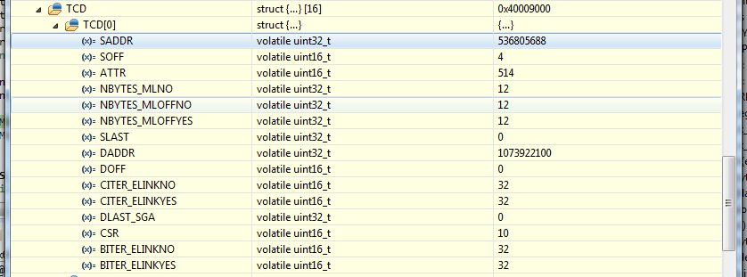
Could you provide the eDMA Channel 0 TCD configuration value (registers value) for DSPI0 TX?
From your code, I find the DSPI0 related pins setting and DSPI0 setting correctly.
I want to make sure the GPIO trigger eDMA will transfer the correct value to SPI0_PUSHR register for SPI0 transmit.
Thank you.
Have a great day,
Ma Hui
-----------------------------------------------------------------------------------------------------------------------
Note: If this post answers your question, please click the Correct Answer button. Thank you!
-----------------------------------------------------------------------------------------------------------------------
- Mark as New
- Bookmark
- Subscribe
- Mute
- Subscribe to RSS Feed
- Permalink
- Report Inappropriate Content
Hi please found the TCD0
And again, if your expert team can build a true code example that compile to prove me it is working, it will be nice.
Thanks
Mikael
- Mark as New
- Bookmark
- Subscribe
- Mute
- Subscribe to RSS Feed
- Permalink
- Report Inappropriate Content
Hi,
Please check my test code attached, which is based on [hello_world] demo located at:
\SDK_2.2_FRDM-K64F\boards\frdmk64f\demo_apps\hello_world
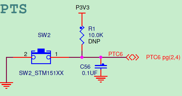
For I test on the FRDM-K64F board, the SW2 pin is using PTC6 pin as EDMA trigger source.
Customer can refer to use PTDx pin as EDMA trigger source.
The test result is below:
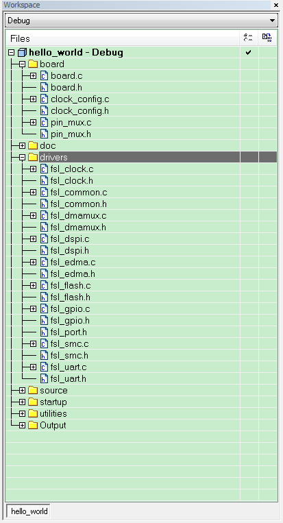
Software structure:
Wish it helps.
Have a great day,
Ma Hui
-----------------------------------------------------------------------------------------------------------------------
Note: If this post answers your question, please click the Correct Answer button. Thank you!
-----------------------------------------------------------------------------------------------------------------------
- Mark as New
- Bookmark
- Subscribe
- Mute
- Subscribe to RSS Feed
- Permalink
- Report Inappropriate Content
Hi
thanks for your example. I'm going to check it.
some questions:
1) how the Rx channel should be configured now ? Do you have an example ?
2) In your example the transfer is four bytes per trigger.
If I need it to be autoreload without interrupt, what I need to modify ? ( in my case each trigger is 12 bytes transfer and each autoreload will be each 32 triggers). Can you help me please ?
thank you very much
- Mark as New
- Bookmark
- Subscribe
- Mute
- Subscribe to RSS Feed
- Permalink
- Report Inappropriate Content
Hi,
1) how the Rx channel should be configured now ? Do you have an example ?
TS:I would recommend to refer the example of MCUXpresso SDK example [edma_transfer] demo, which call the <fsl_dspi_edma.c> driver. The demo located at below folder:
..\SDK_2.2_FRDM-K64F\boards\frdmk64f\driver_examples\dspi\edma_transfer
2) In your example the transfer is four bytes per trigger.
If I need it to be autoreload without interrupt, what I need to modify ? ( in my case each trigger is 12 bytes transfer and each autoreload will be each 32 triggers). Can you help me please ?
TS: The K64 SPI Buffered transmit operation using the transmit first in first out (TX FIFO) with depth of 4 entries. For you are using GPIO to trigger edma transfer will cause problem if there with more bytes need be transfer. The edma move data from memory to SPI0_PUSHR register speed is much faster than SPI actual transfer speed. There will cause the TX FIFO be overwritten before the data was transferred. My conclusion is using GPIO to trigger edma to start SPI TX is not a good choice. The software should keep an eye on SPI TX FIFO status(TFFF) if TX FIFO need more data or not. My suggestion is using GPIO pin to start the SPI transfer, while the edma was triggered by SPI module TX itself. You can set a SPI transfer enable flag at GPIO pin interrupt and when SPI detect this flag will start the SPI transfer automatically with calling <fsl_dspi_edma.c> driver. I still recommend customer to refer the MCUXpresso SDK example [edma_transfer] demo.
Wish it helps.
Have a great day,
Ma Hui
-----------------------------------------------------------------------------------------------------------------------
Note: If this post answers your question, please click the Correct Answer button. Thank you!
-----------------------------------------------------------------------------------------------------------------------
- Mark as New
- Bookmark
- Subscribe
- Mute
- Subscribe to RSS Feed
- Permalink
- Report Inappropriate Content
Thanks for your answer.
All the purpose was to not disturb the CPU with interrupts.
So let's say I use the gpio trigger for the first byte only and then this SPI transfer will trigger the remained frame (so 11 bytes for me).
1) Is it possible ?
2) if yes, so I will need to configure 3 DMA handles (One for gpio trigger, one for spi tx and one for spi rx). Are you agree with that ?
thanks
- Mark as New
- Bookmark
- Subscribe
- Mute
- Subscribe to RSS Feed
- Permalink
- Report Inappropriate Content
Hi,
When each ADC 32 new samples done, the external ADC chip will trigger the GPIO pin to start the SPI transfer.
My suggestion is to use GPIO interrupt to start DSPI0 transfer (clear SPI0_MCR[HALT] bit).
While customer also could use DMA to transfer a 32-bit data to SPI0_MCR register to start DSPI0 transfer.
Then, the SPI will trigger DMA two channels for SPI TX/RX 12 bytes.
When the 12 bytes TX/RX done, the SPI/DMA will trigger the interrupt to refresh DMA two channles TCD configuration for next round transfer.
Have a great day,
Ma Hui
-----------------------------------------------------------------------------------------------------------------------
Note: If this post answers your question, please click the Correct Answer button. Thank you!
-----------------------------------------------------------------------------------------------------------------------
- Mark as New
- Bookmark
- Subscribe
- Mute
- Subscribe to RSS Feed
- Permalink
- Report Inappropriate Content
No no no !!! Maybe I didn't explained you well.
I get ONE gpio trigger PER SAMPLE.
For each sample (or each trigger) I need to transmit 12 bytes through SPI in order to receive the sample. Ideally I hoped to be disturbed by interrupt each 32 samples (because 32 samples in one page in my flash memory.
Keep in mind that I need to work at 48. Kilo samples per seconds, so it is very hard to get one interrupt per sample at this rate.
Please advise on one scenario...
thanks
- Mark as New
- Bookmark
- Subscribe
- Mute
- Subscribe to RSS Feed
- Permalink
- Report Inappropriate Content
Hello Mikael
I have a complete solution for this in the uTasker project, which allows port triggering to write/read SPI sequences without any interrupt overhead. Below are some details and I have attached binary that you can load to a FRDM-K64F to check the behavior.
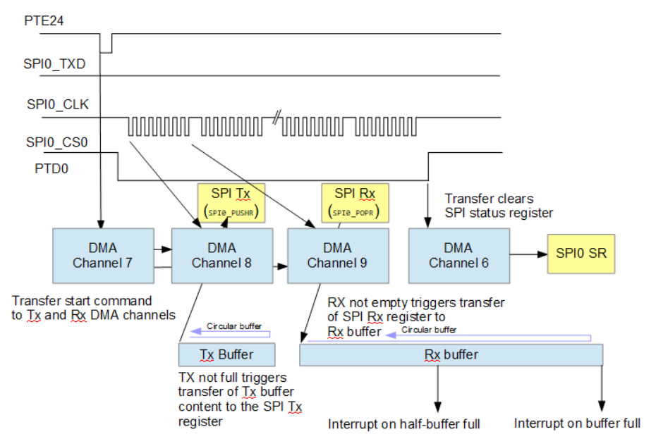
1. If you load the binary to the board you will find a 48kHz PWM output on pin J2-4 (PTC4). By connecting this to J2-20 (PTE-24) it will be used as the port edge DMA trigger (or else you can apply faster clocks to the pin too if you prefer).
SPI0 is used (this has a 4 deep FIFO on Tx and Rx - SPI1 and SPI2 have only 1 deep FIFOs but this is in fact not relevant since the DMA operation is the same for all). This means that SPI0_CS0 can be measured on J2-6 (PTD0), SPI0_SCLK on J2-12 (PTD1), SPI0_SOUT on J2-8 (PTD2). By connecting J2-8 to J2-10 the output can be looped back to the input.
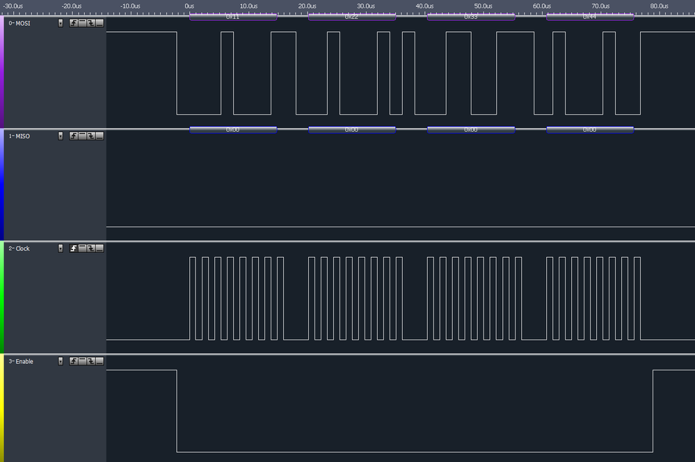
This is what the signals look like (SPI sends 0x01, 0x02, 0x03, etc.)
As seen, the SPI sequence is started by the falling edge of the input.
The received data is stored to a buffer which can be of any size. There is an interrupt when it is half full and when it is completely full and this can be used to retrieve the data from this half while the next is still filling (ping-pong buffer). It is in fact optional since it is also possible to use no interrupts and still successfully receive the data.
2. This is the code used, which makes use of the uTasker DMA driver API which make it very simple to configure and modify to achieve flexible and power ful solutions like this with little effort (it also allows simulation of the operation in the uTasker simulation so that the complete operation can be checked and verified before running it on the HW):
#define DMA_CHANNEL_FOR_CS_END 6 // use DMA channel 6 for CS end trigger
#define DMA_CHANNEL_FOR_PORT_EDGE 7 // use DMA channel 7 for SPI sequence start trigger
#define DMA_CHANNEL_FOR_SPI_TX 8 // use DMA channel 8 for SPI Tx
#define DMA_CHANNEL_FOR_SPI_RX 9 // use DMA channel 9 for SPI Rx
// The SPI Tx data to be sent at each trigger
//
static const unsigned long ulSPI_TX[8] = { // fixed SPI transmission (0x01, 0x02,.. 0x08) with CS asserted throughout the frame
(0x01 | SPI_PUSHR_CONT | SPI_PUSHR_PCS0 | SPI_PUSHR_CTAS_CTAR0),
(0x02 | SPI_PUSHR_CONT | SPI_PUSHR_PCS0 | SPI_PUSHR_CTAS_CTAR0),
(0x03 | SPI_PUSHR_CONT | SPI_PUSHR_PCS0 | SPI_PUSHR_CTAS_CTAR0),
(0x04 | SPI_PUSHR_CONT | SPI_PUSHR_PCS0 | SPI_PUSHR_CTAS_CTAR0),
(0x05 | SPI_PUSHR_CONT | SPI_PUSHR_PCS0 | SPI_PUSHR_CTAS_CTAR0),
(0x06 | SPI_PUSHR_CONT | SPI_PUSHR_PCS0 | SPI_PUSHR_CTAS_CTAR0),
(0x07 | SPI_PUSHR_CONT | SPI_PUSHR_PCS0 | SPI_PUSHR_CTAS_CTAR0),
(0x08 | SPI_PUSHR_EOQ | SPI_PUSHR_PCS0 | SPI_PUSHR_CTAS_CTAR0), // final byte negates CS after transmission
};
static volatile unsigned char ucRxData[128] = {0}; // circular reception buffer (SPi rx data is stored here)
static const unsigned char ucDMA_start = ((DMA_ERQ_ERQ0 << (DMA_CHANNEL_FOR_SPI_TX - 8)) | (DMA_ERQ_ERQ0 << (DMA_CHANNEL_FOR_SPI_RX - 8))); // the value to be written to start the SPI DMA transfer
static const unsigned long ulSPI_clear = (SPI_SR_RFDF | SPI_SR_RFOF | SPI_SR_TFUF | SPI_SR_EOQF | SPI_SR_TCF); // this is written to the SPI status register after the CS negates in order to clear flags and allow subsequent transfers
// Configure the DMA trigger from an input pin edge to start an SPI transfer
//
INTERRUPT_SETUP interrupt_setup; // interrupt configuration parameters
interrupt_setup.int_port = PORTE; // the port that the interrupt input is on
interrupt_setup.int_port_bits = PORTE_BIT24; // PTE24
interrupt_setup.int_port_sense = (IRQ_FALLING_EDGE | PULLUP_ON | PORT_DMA_MODE); // DMA on falling edge
interrupt_setup.int_handler = 0; // no interrupt handler when using DMA
fnConfigureInterrupt((void *)&interrupt_setup); // configure interrupt/DMA
// Configure the DMA trigger from an input pin edge to clear the SPI status register
//
interrupt_setup.int_port = PORTD; // the port that the interrupt input is on
interrupt_setup.int_port_bits = PORTD_BIT0; // PTD0, which is the SPI CS output
interrupt_setup.int_port_sense = (IRQ_RISING_EDGE | PULLUP_ON | PORT_DMA_MODE | PORT_KEEP_PERIPHERAL); // DMA on rising edge (keep CS peripheral to trigger on the end of a transfer9
fnConfigureInterrupt((void *)&interrupt_setup); // configure interrupt/DMA
// Initialise SPI interface
//
POWER_UP_ATOMIC(6, SPI0);
_CONFIG_PERIPHERAL(D, 0, (PD_0_SPI0_PCS0 | PORT_SRE_FAST | PORT_DSE_HIGH));
_CONFIG_PERIPHERAL(D, 1, (PD_1_SPI0_SCK | PORT_SRE_FAST | PORT_DSE_HIGH));
_CONFIG_PERIPHERAL(D, 2, (PD_2_SPI0_SOUT | PORT_SRE_FAST | PORT_DSE_HIGH));
_CONFIG_PERIPHERAL(D, 3, (PD_3_SPI0_SIN));
SPI0_MCR = (SPI_MCR_MSTR | SPI_MCR_DCONF_SPI | SPI_MCR_CLR_RXF | SPI_MCR_CLR_TXF | SPI_MCR_PCSIS_CS0 | SPI_MCR_PCSIS_CS1 | SPI_MCR_PCSIS_CS2 | SPI_MCR_PCSIS_CS3 | SPI_MCR_PCSIS_CS4 | SPI_MCR_PCSIS_CS5);
SPI0_RSER = (SPI_SRER_TFFF_DIRS | SPI_SRER_TFFF_RE | SPI_SRER_RFDF_DIRS | SPI_SRER_RFDF_RE); // enable rx and tx DMA requests
SPI0_CTAR0 = (SPI_CTAR_DBR | SPI_CTAR_FMSZ_8 | SPI_CTAR_PDT_7 | SPI_CTAR_BR_4 | SPI_CTAR_CPHA | SPI_CTAR_CPOL); // for 60MHz bus, 15MHz speed and 120ns min de-select time
// Configure SPI TX DMA to transfer the content of ulSPI_TX[] on each DMA trigger
//
fnConfigDMA_buffer(DMA_CHANNEL_FOR_SPI_TX, DMAMUX_CHCFG_SOURCE_SPI0_TX, sizeof(ulSPI_TX), (void *)ulSPI_TX, (void *)SPI0_PUSHR_ADDR, (DMA_DIRECTION_OUTPUT | DMA_LONG_WORDS | DMA_SINGLE_CYCLE), 0, 0); // source is the tx buffer and destination is the SPI transmit register without interrupts (free-running)
// Configure SPI RX DMA to save reception continuously to ucRxData[] (with optional interrupt call back at haf and complete buffer)
//
fnConfigDMA_buffer(DMA_CHANNEL_FOR_SPI_RX, DMAMUX_CHCFG_SOURCE_SPI0_RX, sizeof(ucRxData), (void *)SPI0_POPR_ADDR, (void *)ucRxData, (DMA_DIRECTION_INPUT | DMA_BYTES | DMA_HALF_BUFFER_INTERRUPT), spi_half_buffer, PRIORITY_DMA9); // source is the SPI reception register and destination is the input buffer with interrupt at half- and full buffer
// Configure the falling edge port input to a DMA cycle
//
fnConfigDMA_buffer(DMA_CHANNEL_FOR_PORT_EDGE, DMAMUX0_CHCFG_SOURCE_PORTE, sizeof(ucDMA_start), (void *)&ucDMA_start, (void *)(((unsigned char *)DMA_ERQ_ADDR) + 1), (DMA_FIXED_ADDRESSES | DMA_BYTES), 0, 0); // use DMA channel without any interrupts (free-runnning)
fnDMA_BufferReset(DMA_CHANNEL_FOR_PORT_EDGE, DMA_BUFFER_START); // enable the DMA operation - a falling edge on the port will now trigger SPI Tx and Rx DMA operation
// Configure a rising edge port input (CS line negation) to reset the SPI status register so that the following cycle can operate
//
fnConfigDMA_buffer(DMA_CHANNEL_FOR_CS_END, DMAMUX0_CHCFG_SOURCE_PORTD, sizeof(ulSPI_clear), (void *)&ulSPI_clear, (void *)SPI0_SR_ADDR, (DMA_FIXED_ADDRESSES | DMA_LONG_WORDS), 0, 0); // use DMA channel without any interrupts (free-runnning)
fnDMA_BufferReset(DMA_CHANNEL_FOR_CS_END, DMA_BUFFER_START); // enable the DMA operation - a rising edge on the port will now a clear of the SPI status register
// From this point the SPI operation runs driven exclusively by DMA and no CPU intervention (the operation continues even when the debugger pauses the CPU operation)
//
// Optional interrupt call back handler
//
static void spi_half_buffer(void)
{
// This is called each time the SPI Rx buffer is half-full or full so that the previous half buffer content can be retrieved while the next half is still being filled
//
}
3. This diagram shows how 4 DMA channels are required, whereby there is a slight complication since it is also necessary to clear the SPI status register flags after each transfer so that it can continue (otherwise only 3 would have been necessary)
Conclusion:
- Is is very simple to achieve extremely efficient SPI operation of this type, allowing very high speed sampling rates without CPU intervention. By setting a large Rx buffer the CPU can read and process the data at leisure without risk of overruns.
Final notes: the attached binary also has USB-CDC on the USB and a TCP/IP stack operation on the Ethernet (IP 192.168.0.5) to show that the high speed SPI sampling doesn't interfere with the other operations.
On the debug interface (OpenSDA VCOM at 115200 Baud or the USB-CDC interface) there is a command line menu. In the I/O menu you can view memory.
The command "md 1fff02cc b 128" displays the content of the Rx buffer (the address was found in the map file) so that you can check received data if you loop back the SPI Tx to see that it fills up as the triggers arrive.
This is available as turn-key solution in the uTasker project and runs on any Kinetis part with DSPI and eDMA.
Please contact me in case you would like the code or advice on how to adapt yours to achieve your requirement.
Regards
Mark
Kinetis: http://www.utasker.com/kinetis.html
k64:
- http://www.utasker.com/kinetis/FRDM-K64F.html
- http://www.utasker.com/kinetis/TWR-K64F120M.html
- http://www.utasker.com/kinetis/TEENSY_3.5.html
- http://www.utasker.com/kinetis/Hexiwear-K64F.html
Faster and cheaper project development....
- Mark as New
- Bookmark
- Subscribe
- Mute
- Subscribe to RSS Feed
- Permalink
- Report Inappropriate Content
Sorry, now it is OK.
Let me check it.
Thanks
- Mark as New
- Bookmark
- Subscribe
- Mute
- Subscribe to RSS Feed
- Permalink
- Report Inappropriate Content
Sorry but I dont see the attached file.
thanks
Mikael
- Mark as New
- Bookmark
- Subscribe
- Mute
- Subscribe to RSS Feed
- Permalink
- Report Inappropriate Content
Hi Mikael,
I am working on a project for your reference now.
It will take some time and thank you for the patience.
I will post that project when it was tested. Thanks.
Have a great day,
Ma Hui
-----------------------------------------------------------------------------------------------------------------------
Note: If this post answers your question, please click the Correct Answer button. Thank you!
-----------------------------------------------------------------------------------------------------------------------
- Mark as New
- Bookmark
- Subscribe
- Mute
- Subscribe to RSS Feed
- Permalink
- Report Inappropriate Content
Hi ,
Thanks for your response.
We had the same discussion two months ago and you didn't found any issues.
https://community.nxp.com/thread/456058
I'm going to check you the TCDx values, and will provide them as soon as possible.
But anyway, are you able to provide me an example working on eval board (for example) to prove me it can work ?
A simple example, with a push button as trigger, and SPI Tx on K64 ...
My project is blocked since 2 months.
Thanks.
