- Forums
- Product Forums
- General Purpose MicrocontrollersGeneral Purpose Microcontrollers
- i.MX Forumsi.MX Forums
- QorIQ Processing PlatformsQorIQ Processing Platforms
- Identification and SecurityIdentification and Security
- Power ManagementPower Management
- Wireless ConnectivityWireless Connectivity
- RFID / NFCRFID / NFC
- Advanced AnalogAdvanced Analog
- MCX Microcontrollers
- S32G
- S32K
- S32V
- MPC5xxx
- Other NXP Products
- S12 / MagniV Microcontrollers
- Powertrain and Electrification Analog Drivers
- Sensors
- Vybrid Processors
- Digital Signal Controllers
- 8-bit Microcontrollers
- ColdFire/68K Microcontrollers and Processors
- PowerQUICC Processors
- OSBDM and TBDML
- S32M
- S32Z/E
-
- Solution Forums
- Software Forums
- MCUXpresso Software and ToolsMCUXpresso Software and Tools
- CodeWarriorCodeWarrior
- MQX Software SolutionsMQX Software Solutions
- Model-Based Design Toolbox (MBDT)Model-Based Design Toolbox (MBDT)
- FreeMASTER
- eIQ Machine Learning Software
- Embedded Software and Tools Clinic
- S32 SDK
- S32 Design Studio
- GUI Guider
- Zephyr Project
- Voice Technology
- Application Software Packs
- Secure Provisioning SDK (SPSDK)
- Processor Expert Software
- Generative AI & LLMs
-
- Topics
- Mobile Robotics - Drones and RoversMobile Robotics - Drones and Rovers
- NXP Training ContentNXP Training Content
- University ProgramsUniversity Programs
- Rapid IoT
- NXP Designs
- SafeAssure-Community
- OSS Security & Maintenance
- Using Our Community
-
- Cloud Lab Forums
-
- Knowledge Bases
- ARM Microcontrollers
- i.MX Processors
- Identification and Security
- Model-Based Design Toolbox (MBDT)
- QorIQ Processing Platforms
- S32 Automotive Processing Platform
- Wireless Connectivity
- CodeWarrior
- MCUXpresso Suite of Software and Tools
- MQX Software Solutions
- RFID / NFC
- Advanced Analog
-
- NXP Tech Blogs
- Home
- :
- CodeWarrior
- :
- CodeWarrior Development Tools
- :
- Re: DDR validation failed
DDR validation failed
- Subscribe to RSS Feed
- Mark Topic as New
- Mark Topic as Read
- Float this Topic for Current User
- Bookmark
- Subscribe
- Mute
- Printer Friendly Page
DDR validation failed
- Mark as New
- Bookmark
- Subscribe
- Mute
- Subscribe to RSS Feed
- Permalink
- Report Inappropriate Content
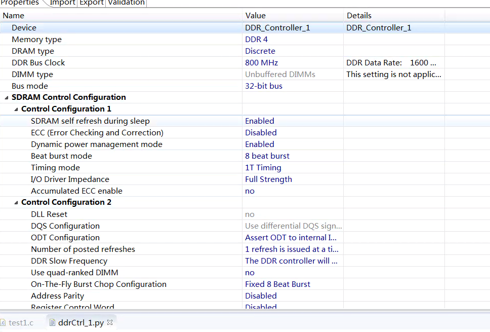
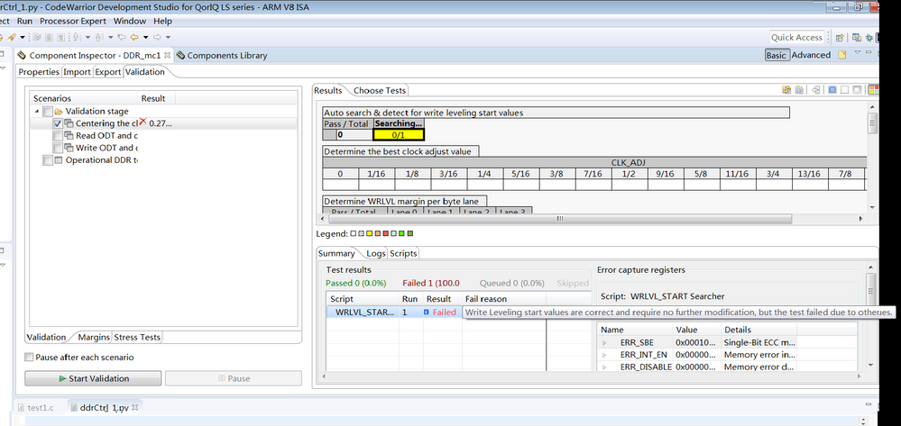
What could be the cause of DDR validation write leveing failed, and how to solve it? The configuration and error information of DDR are as follows:
- Mark as New
- Bookmark
- Subscribe
- Mute
- Subscribe to RSS Feed
- Permalink
- Report Inappropriate Content
The attachment is part of ddr schematic diagram, ddr datasheet and ddr validation report。DQ map configuration is 0x1. Only the CL-nRCD-nRP timing parameter in the ddr datasheet is 22. Because the emulator is used, clk to DQS Skew is not filled in.The following are the register configuration values generated by the QCVS tool:
#define DDRmc1_CS0_BNDS VALUE_OF(0x7F)
#define DDRmc1_CS1_BNDS VALUE_OF(0x008000BF)
#define DDRmc1_CS0_CONFIG VALUE_OF(0x80010512)
#define DDRmc1_CS1_CONFIG VALUE_OF(0x0202)
#define DDRmc1_CS0_CONFIG_2 VALUE_OF(0x00)
#define DDRmc1_CS1_CONFIG_2 VALUE_OF(0x00)
#define DDRmc1_CS2_BNDS VALUE_OF(0x00C000FF)
#define DDRmc1_CS3_BNDS VALUE_OF(0x0100013F)
#define DDRmc1_CS2_CONFIG VALUE_OF(0x0202)
#define DDRmc1_CS3_CONFIG VALUE_OF(0x0202)
#define DDRmc1_CS2_CONFIG_2 VALUE_OF(0x00)
#define DDRmc1_CS3_CONFIG_2 VALUE_OF(0x00)
#define DDRmc1_TIMING_CFG_3 VALUE_OF(0x11562000)
#define DDRmc1_TIMING_CFG_0 VALUE_OF(0x8055000C)
#define DDRmc1_TIMING_CFG_1 VALUE_OF(0x6B6A0C42)
#define DDRmc1_TIMING_CFG_2 VALUE_OF(0x0048D11C)
#define DDRmc1_SDRAM_CFG VALUE_OF(0x452C0000)
#define DDRmc1_SDRAM_CFG2 VALUE_OF(0x00401010)
#define DDRmc1_MODE_1 VALUE_OF(0x01010250)
#define DDRmc1_MODE_2 VALUE_OF(0x00)
#define DDRmc1_MODE_3 VALUE_OF(0x00)
#define DDRmc1_MODE_4 VALUE_OF(0x00)
#define DDRmc1_MODE_5 VALUE_OF(0x00)
#define DDRmc1_MODE_6 VALUE_OF(0x00)
#define DDRmc1_MODE_7 VALUE_OF(0x00)
#define DDRmc1_MODE_8 VALUE_OF(0x00)
#define DDRmc1_MODE_CONTROL VALUE_OF(0x00)
#define DDRmc1_INTERVAL VALUE_OF(0x18600618)
#define DDRmc1_MEM_INIT_VALUE VALUE_OF(0xDEADBEEF)
#define DDRmc1_CLK_CTRL VALUE_OF(0x02800000)
#define DDRmc1_WRLVL_CNTL VALUE_OF(0x86750608)
#define DDRmc1_WRLVL_CNTL_2 VALUE_OF(0x07080705)
#define DDRmc1_WRLVL_CNTL_3 VALUE_OF(0x05050500)
#define DDRmc1_INIT_ADDR VALUE_OF(0x00)
#define DDRmc1_INIT_EXT_ADDR VALUE_OF(0x00)
#define DDRmc1_TIMING_CFG_4 VALUE_OF(0x01)
#define DDRmc1_TIMING_CFG_5 VALUE_OF(0x05401400)
#define DDRmc1_ZQ_CNTL VALUE_OF(0x8A090705)
#define DDRmc1_RCW_1 VALUE_OF(0x00)
#define DDRmc1_RCW_2 VALUE_OF(0x00)
#define DDRmc1_CDR_1 VALUE_OF(0x80040000)
#define DDRmc1_CDR_2 VALUE_OF(0xA181)
#define DDRmc1_SDRAM_CFG_3 VALUE_OF(0x00)
#define DDRmc1_TIMING_CFG_6 VALUE_OF(0x00)
#define DDRmc1_TIMING_CFG_7 VALUE_OF(0x23300000)
#define DDRmc1_TIMING_CFG_8 VALUE_OF(0x0D115600)
#define DDRmc1_DESKEW_CNTL VALUE_OF(0x00)
#define DDRmc1_DQ_MAP0 VALUE_OF(0x04104104)
#define DDRmc1_DQ_MAP1 VALUE_OF(0x04104000)
#define DDRmc1_DQ_MAP2 VALUE_OF(0x00)
#define DDRmc1_DQ_MAP3 VALUE_OF(0x00)
#define DDRmc1_RCW_3 VALUE_OF(0x00)
#define DDRmc1_RCW_4 VALUE_OF(0x00)
#define DDRmc1_RCW_5 VALUE_OF(0x00)
#define DDRmc1_RCW_6 VALUE_OF(0x00)
#define DDRmc1_MODE_9 VALUE_OF(0x0400)
#define DDRmc1_MODE_10 VALUE_OF(0x04800000)
#define DDRmc1_MODE_11 VALUE_OF(0x00)
#define DDRmc1_MODE_12 VALUE_OF(0x00)
#define DDRmc1_MODE_13 VALUE_OF(0x00)
#define DDRmc1_MODE_14 VALUE_OF(0x00)
#define DDRmc1_MODE_15 VALUE_OF(0x00)
#define DDRmc1_MODE_16 VALUE_OF(0x00)
#define DDRmc1_ERR_DISABLE VALUE_OF(0x00)
#define DDRmc1_ERR_INT_EN VALUE_OF(0x00)
#define DDRmc1_ERR_SBE VALUE_OF(0x00010000)
- Mark as New
- Bookmark
- Subscribe
- Mute
- Subscribe to RSS Feed
- Permalink
- Report Inappropriate Content
In DDRv Report ERR_DETECT[ACE] is set, ERR_SBE[SBEC] is set.
For ECC failures during the operation, please configure DDR properties according to DDR datasheet, use the validation section of QCVS to optimize the setting. if ECC persist with optimized setting then there may be a HW issue (check the AN5097 for the layout guidelines).
- Mark as New
- Bookmark
- Subscribe
- Mute
- Subscribe to RSS Feed
- Permalink
- Report Inappropriate Content
What attributes do you generally need to configure according to the DDR datasheet? We are now using QCVS for validation, but the first item cannot be passed and this kind of error is reported. In our QCVS configuration, ECC is prohibited.
- Mark as New
- Bookmark
- Subscribe
- Mute
- Subscribe to RSS Feed
- Permalink
- Report Inappropriate Content
In the CCS console, please type "log v", then connect to the target board again, the low level CCS log will be printed in the console, please provide this log.
- Mark as New
- Bookmark
- Subscribe
- Mute
- Subscribe to RSS Feed
- Permalink
- Report Inappropriate Content
how to open CCS console,thanks
- Mark as New
- Bookmark
- Subscribe
- Mute
- Subscribe to RSS Feed
- Permalink
- Report Inappropriate Content
CCS is at the right bottom of the task bar, please double click to open it.
- Mark as New
- Bookmark
- Subscribe
- Mute
- Subscribe to RSS Feed
- Permalink
- Report Inappropriate Content
Please configure the Properties panel according to the DDR datasheet. If there is DDR SPD on your target board, please create QCVS DDR project with reading from SPD method. RCW on the target board should be valid. Enter MCK to DQS skews in the DDR wizard, verify the DQn_MAP registers are correct.
In the Summary panel in CodeWarrior IDE, you could check some registers value, please check whether ERR_DETECT[ACE] is set, and whether ERR_SBE[SBEC] is set.
If ERR_DETECT[ACE] is set, please refer to my last reply in https://community.nxp.com/message/1208703?commentID=1208703#comment-1208703

