- Forums
- Product Forums
- General Purpose MicrocontrollersGeneral Purpose Microcontrollers
- i.MX Forumsi.MX Forums
- QorIQ Processing PlatformsQorIQ Processing Platforms
- Identification and SecurityIdentification and Security
- Power ManagementPower Management
- Wireless ConnectivityWireless Connectivity
- RFID / NFCRFID / NFC
- Advanced AnalogAdvanced Analog
- MCX Microcontrollers
- S32G
- S32K
- S32V
- MPC5xxx
- Other NXP Products
- S12 / MagniV Microcontrollers
- Powertrain and Electrification Analog Drivers
- Sensors
- Vybrid Processors
- Digital Signal Controllers
- 8-bit Microcontrollers
- ColdFire/68K Microcontrollers and Processors
- PowerQUICC Processors
- OSBDM and TBDML
- S32M
- S32Z/E
-
- Solution Forums
- Software Forums
- MCUXpresso Software and ToolsMCUXpresso Software and Tools
- CodeWarriorCodeWarrior
- MQX Software SolutionsMQX Software Solutions
- Model-Based Design Toolbox (MBDT)Model-Based Design Toolbox (MBDT)
- FreeMASTER
- eIQ Machine Learning Software
- Embedded Software and Tools Clinic
- S32 SDK
- S32 Design Studio
- GUI Guider
- Zephyr Project
- Voice Technology
- Application Software Packs
- Secure Provisioning SDK (SPSDK)
- Processor Expert Software
- Generative AI & LLMs
-
- Topics
- Mobile Robotics - Drones and RoversMobile Robotics - Drones and Rovers
- NXP Training ContentNXP Training Content
- University ProgramsUniversity Programs
- Rapid IoT
- NXP Designs
- SafeAssure-Community
- OSS Security & Maintenance
- Using Our Community
-
- Cloud Lab Forums
-
- Knowledge Bases
- ARM Microcontrollers
- i.MX Processors
- Identification and Security
- Model-Based Design Toolbox (MBDT)
- QorIQ Processing Platforms
- S32 Automotive Processing Platform
- Wireless Connectivity
- CodeWarrior
- MCUXpresso Suite of Software and Tools
- MQX Software Solutions
- RFID / NFC
- Advanced Analog
-
- NXP Tech Blogs
- Home
- :
- i.MX处理器
- :
- i.MX处理器知识库
- :
- System Controller Firmware 101 - Pad configuration service
System Controller Firmware 101 - Pad configuration service
System Controller Firmware 101 - Pad configuration service
System Controller Firmware 101 - Pad configuration service
This document explains the pad implementation and its relationship with the System Controller Firmware pad configuration service.
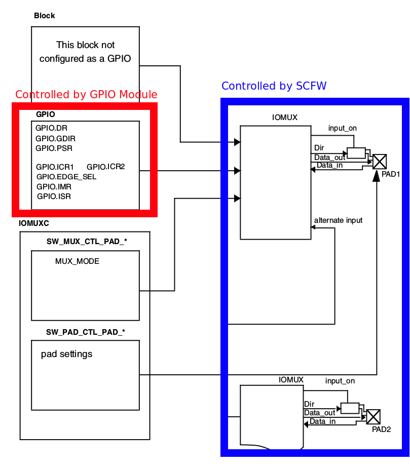
There are two components to pad configuration in the SCFW, there are the modules that generate the signals that will ultimately appear on the physical pad, let's say GPIO/Ethernet/I2C/UART etc... and then there is the part that configures the muxing of the pad (what signal is going to be outputted through the specific pad), the drive strength of the pad, pull selection, etc, this is the part that the SCFW pad service configures.
Introduction
The i.MX8 has three types of I/Os:
- 1.8V only I/Os
- 3.3V only I/Os
- 1.8V / 3.3V I/Os Dual Voltage I/Os
Note: USB High Speed Inter-Chip (HSIC) and Ethernet interfaces have specific integration schemes with dedicated features.
They are a modified versions of the above I/O types.
- HSIC are a special kind of I/O modified to sustain 480Mbps data rates
- ENET I/Os are modified versions of Dual Voltage I/Os to support 2.5V operations
All of these I/Os have "common features" and "technology specific features" which depend on the type of I/O and the chip manufacturing process (FDSOI in the i.MX8QM case)
I/O common features
Muxing capability of up to 4 signals
Each Pad can have up to 4 signals, only one signal can be present in the pad.
To select the signal that will output on the pad simply look at the Pinmux spreadsheet and use the desired alternative, for instance in the following image SCU_GPIO0_00 has 3 options, SCU_GPIO (ALT0 - GPIO controlled directly by the SCU), SCU_UART0_RX (ALT1 - SCU UART receiver) or LSIO_GPIO0_IO28 (ALT3 - Low speed I/O GPIO).
Pads without GPIO functionality (i.e. without the GPIO option in the pinmux spreadsheet) are implemented for one purpose only, these pins are connected directly to the module that drives them and they feature their own physical interface. Examples are XTAL pins, DDR pins and SCU PMIC interface (shown above).
Mode of operation
All GPIO types support four modes of operation:
Normal mode
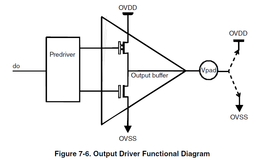
Data is being driven directly to the pad (an internal signal of 1 shows in the pad as a 1 and vice-versa) and the pad works either as an output or as an input but not both at the same time. The output buffer while on this mode looks like this:
 Open drain
Data is being driven through an open drain configuration, the output on the pad switches between 0 and high-z. The pad works either as an output or as an input but not both at the same time, e.g. if the Output Buffer is enabled the Input Buffer is disabled. This is how the output buffer looks like on Open drain mode:
 Open drain and input
Output buffer acts as in open drain mode but with the input buffer enabled regardless of the output buffer state (enabled/disabled), this allows to simultaneously read the signal at the pad while driving it.
Output and input
Output buffer acts as in normal mode but with the input buffer enabled regardless of the output buffer state (enabled/disabled), this allows to read the signal at the pad while driving it.
Wake-up capability
Each I/O can be configured to wake-up the device, the following configuration options are available:
OFF
I/O cannot wake-up the system
Low detect
Generate wake-up event when the pad remains in low-level
High detect
Generate wake-up event when the pad remains in high-level
Rising edge
Generate wake-up event on rising edge detection
Falling edge
Generate wake-up event on falling edge detection
Technology specific features
Some of the available features for each pad depend on two factors:
- Chip manufacturing process (FDSOI or LPP)
- I/O type (1.8V, 3.3V or Dual Voltage)
The i.MX8QM is manufactured using FDSOI technology and it features all of the three available I/O types.
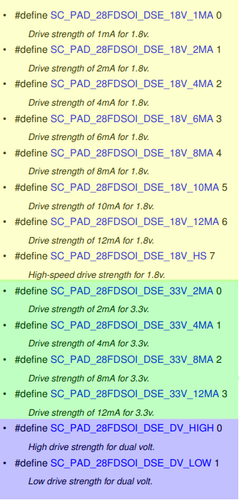
Drive strength
Drive strength options vary within I/O types and chip manufacturing options.
The available options for a FDSOI chip are:
1.8V Drive strength options | 3.3V Drive strength options | Dual Voltage drive strength options |
Drive strength of 1mA | Drive strength of 2mA | Low drive strength (50 ohms) |
Drive strength of 2mA | Drive strength of 4mA | High drive strength (33 ohms) |
Drive strength of 4mA | Drive strength of 8mA | |
Drive strength of 6mA | Drive strength of 12mA | |
Drive strength of 8mA | ||
Drive strength of 10mA | ||
Drive strength of 12mA | ||
High-speed drive strength |
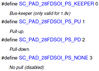
Pull Select
The pull select available options are almost the same for all I/O types (1.8V being the exception) and they also depend on chip manufacturing process.
The available options for a FDSOI chip are:
Pull select options for FDSOI |
Bus-keeper (only available for 1.8V) |
Pull-up |
Pull-down |
No Pull (Disabled) |
A bus-keeper or bus-holder is used to keep the last state on the bus. In normal operation it makes no difference, but once the bus is tri-stated it keeps the last logic level in the bus to prevent the bus from floating.
Compensation
The compensation feature is only available on Dual Voltage I/Os.
Dual Voltage I/Os have a different implementation, they require:
- Voltage reference generator - which provides a voltage reference to the supply detector and compensation cell
- Supply detector - detects automatically whether the I/O is being supplied with 1.8V or 3.3V and broadcasts this information to compensation cell and I/O
- Compensation cell - adjusts drive strength of dual voltage I/Os depending on Process Voltage and Temperature (PVT) conditions.
The default configuration takes care of adjusting this parameters and no further modifications are required.
Pad configuration service SCFW API
Mux selection
The very first function that needs to be called to configure a pad is:
sc_err_t sc_pad_set_mux(sc_ipc_t ipc, sc_pad_t pad, uint8_t mux, sc_pad_config_t config, sc_pad_iso_t iso);This function takes care of configuring the muxing alternative and setting the common features, its parameters are:
- ipc - The Inter Processor Communication (IPC) channel that you will use to communicate with the SCU. You need to call sc_ipc_open to obtain it.
- pad - The pad you want to configure, the different pad definitions are in imx8qm_pads.h, this is basically the same list that is included in the scfw_api_qm.pdf document (page 27 Chapter 5 Pad List) and it also mimics the Pinmux excel sheet.
- mux - The mux setting that you require, basically Alt0 -> 0, Alt1 -> 1, Alt2 -> 2 and Alt3-> 3, the pinmux spreadsheet contains the required information (take a look at I/O common features above).
- config - Used to select the desired mode of operation (take a look at I/O common features above), the available options are declared under sc_pad_config_t
Normal mode - SC_PAD_CONFIG_NORMAL
Open Drain mode - SC_PAD_CONFIG_OD
Open Drain and input - SC_PAD_CONFIG_OD_IN
Output and input - SC_PAD_CONFIG_OUT_IN
- iso - This is the low-power isolation configuration (take a look at I/O common features above). The available options are declared under sc_pad_iso_t
ISO_OFF - SC_PAD_ISO_OFF
ISO_EARLY - SC_PAD_ISO_EARLY
ISO_LATE - SC_PAD_ISO_LATE
ISO_ON - SC_PAD_ISO_ON
For instance to configure M40_I2C0_SCL with its UART alternative in normal mode with low-power isolation off, the call would look like this:
sc_pad_set_mux(ipc, SC_P_M40_I2C0_SCL, 1, SC_PAD_CONFIG_NORMAL, SC_PAD_ISO_OFF);Pad configuration
To configure drive strength and pull select options the technology specific functions need to be used (FDSOI for i.MX8QM):
sc_pad_set_gp is being used by our Linux team because it admits the passing of the configuration parameters as a single value and this eases the handling on the device tree, but you should aim to use the technology specific functions.
sc_err_t sc_pad_set_gp_28fdsoi(sc_ipc_t ipc, sc_pad_t pad, sc_pad_28fdsoi_dse_t dse, sc_pad_28fdsoi_ps_t ps);This function takes care of configuring the drive strength (DSE) and pull select settings (PS) for the specified pad, here is a break down of the parameters it uses:
- ipc - The Inter Processor Communication (IPC) channel that you will use to communicate with the SCU. You need to call sc_ipc_open to obtain it.
- pad - The pad you want to configure, the different pad definitions are in imx8qm_pads.h, this is basically the same list that is included in the scfw_api_qm.pdf document (page 27 Chapter 5 Pad List) and it also mimics the Pinmux excel sheet.
- dse - The desired drive strength configuration (see Technology specific features above). DSE settings depend on the I/O type being used, the available options for each I/O type are defined under sc_pad_28fdsoi_dse_t:
ENET pads capable of operating at 2.5V are a subset of dual voltage I/Os, the dse options available for these pads are the same as normal dual voltage I/Os. i.e. High drive and low drive.
- ps - The desired pull select configuration (see Technology specific features above). The available options are defined under sc_pad_28fdsoi_ps_t:
To determine whether a GPIO pad is 1.8V, 3.3V or Dual Voltage one can look at the pinmux spread sheet, the supply for the pad will indicate what implementation of the GPIO is used. For instance:
- pads under VDD_SIM_1P8_3P3 are Dual voltage I/Os
- pads under VDD_SCU_1P8 are 1.8V I/Os
- pads under VDD_ADC_3P3 are 3.3V I/Os
taking the same example as above we could configure the M40_I2C0_SCL as follows:
sc_pad_set_gp_28fdsoi(ipc, SC_P_M40_I2C0_SCL, SC_PAD_28FDSOI_DSE_DV_LOW, SC_PAD_28FDSOI_PS_NONE);Configuration under Linux
Linux configures pads through the device tree, the full documentation of the binding is under Documentation/devicetree/bindings/pinctrl/fsl,imx8qxp-pinctrl.txt. but here is an extract:
* Freescale i.MX8QXP IOMUX Controller
Required properties:
- compatible: "fsl,imx8qxp-iomuxc"
- fsl,pins: each entry consists of 2 integers. Its format is
<pin_id pin_config>.
pin_config definition:
- i.MX8QXP have different pad types, please refer to below pad
register definitions, the pinctrl driver will just write the
pin_config into the hardware register.The driver uses the following API:
sc_err_t sc_pad_set_gp (sc_ipc_t ipc, sc_pad_t pad, uint32_t ctrl) Instead of configuring each parameter individually as done with sc_pad_set_gp_28fdsoi it configures the pad as if writing to a register, the bitfield format is under the binding documentation but it is as follows:
struct _hw_pad_iomux_bitfields0
{
uint32_t GP : 19; /*!< [18:0] GP controls. */
uint32_t WAKEUP : 3; /*!< [21:19] Wakeup controls. */
uint32_t WAKEUP_ENB : 1; /*!< [22] Wakeup write enable. */
uint32_t LPCONFIG : 2; /*!< [24:23] Low-power config. */
uint32_t CONFIG : 2; /*!< [26:25] Config. */
uint32_t IFMUX : 3; /*!< [29:27] Mux. */
uint32_t GP_ENB : 1; /*!< [30] GP write enable. */
uint32_t IFMUX_ENB : 1; /*!< [31] Mux write enable. */
} B;
All the configurations mentioned above can be configured, but they are done in a single pass, e.g. Muxing, Configuration (Norma, Open Drive, etc...), Wakeup control, and GP controls are for Pull Select Drive Strenght etc... Check the Reference Manual Chapter for IOMUXD for the register definition for each pad.
References
For more details refer to the sc_fw_api.pdf document:
- Chapter 1.3.3 Pad Configuration Service
- Chapter 6 Pad List
- Chapter 9.3 (SVC) Pad Service


