- Forums
- Product Forums
- General Purpose MicrocontrollersGeneral Purpose Microcontrollers
- i.MX Forumsi.MX Forums
- QorIQ Processing PlatformsQorIQ Processing Platforms
- Identification and SecurityIdentification and Security
- Power ManagementPower Management
- Wireless ConnectivityWireless Connectivity
- RFID / NFCRFID / NFC
- Advanced AnalogAdvanced Analog
- MCX Microcontrollers
- S32G
- S32K
- S32V
- MPC5xxx
- Other NXP Products
- S12 / MagniV Microcontrollers
- Powertrain and Electrification Analog Drivers
- Sensors
- Vybrid Processors
- Digital Signal Controllers
- 8-bit Microcontrollers
- ColdFire/68K Microcontrollers and Processors
- PowerQUICC Processors
- OSBDM and TBDML
- S32M
- S32Z/E
-
- Solution Forums
- Software Forums
- MCUXpresso Software and ToolsMCUXpresso Software and Tools
- CodeWarriorCodeWarrior
- MQX Software SolutionsMQX Software Solutions
- Model-Based Design Toolbox (MBDT)Model-Based Design Toolbox (MBDT)
- FreeMASTER
- eIQ Machine Learning Software
- Embedded Software and Tools Clinic
- S32 SDK
- S32 Design Studio
- GUI Guider
- Zephyr Project
- Voice Technology
- Application Software Packs
- Secure Provisioning SDK (SPSDK)
- Processor Expert Software
- Generative AI & LLMs
-
- Topics
- Mobile Robotics - Drones and RoversMobile Robotics - Drones and Rovers
- NXP Training ContentNXP Training Content
- University ProgramsUniversity Programs
- Rapid IoT
- NXP Designs
- SafeAssure-Community
- OSS Security & Maintenance
- Using Our Community
-
- Cloud Lab Forums
-
- Knowledge Bases
- ARM Microcontrollers
- i.MX Processors
- Identification and Security
- Model-Based Design Toolbox (MBDT)
- QorIQ Processing Platforms
- S32 Automotive Processing Platform
- Wireless Connectivity
- CodeWarrior
- MCUXpresso Suite of Software and Tools
- MQX Software Solutions
- RFID / NFC
- Advanced Analog
-
- NXP Tech Blogs
- Home
- :
- ARM Microcontrollers
- :
- Kinetis Microcontrollers Knowledge Base
- :
- IRDA bit banging on FRDM-KE02Z
IRDA bit banging on FRDM-KE02Z
- Subscribe to RSS Feed
- Mark as New
- Mark as Read
- Bookmark
- Subscribe
- Printer Friendly Page
- Report Inappropriate Content
IRDA bit banging on FRDM-KE02Z
IRDA bit banging on FRDM-KE02Z
Hello all,
So, this time there is a query on implementing IRDA communication by bit banging the GPIOs. So, I come up with an experiment to do so. Before that, why bit banging when KE02 supports IR communication right away by using FTM at TX and ACMP at RX? something similar to this Implementing infrared functions on UART0 with FRDM-KE02Z platform.
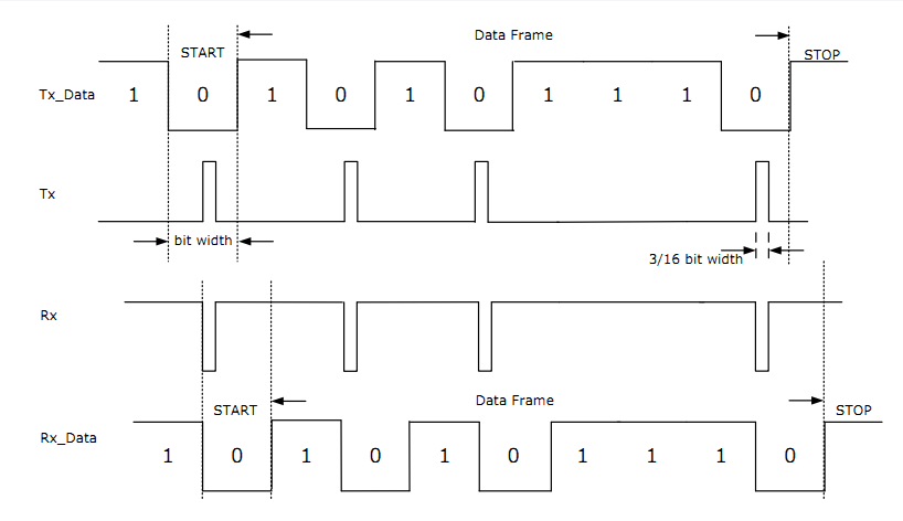
The answer lies in the waveform attached. In the code from the above discussion, the PWM modulation is performed on FTM channel for transmission, while the communication that customer required was different and the waveform required is the one attached.
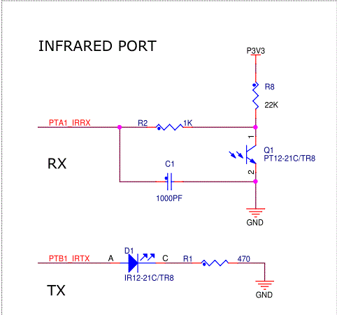
Note that the IRDA transmitter on FRDM-KE02Z is connected to UART0. But, in the attached code, UART0 is not configured for IRDA_TX. while ACMP is used for RX.
This post is intended to be a reference to those who want to implement IRDA with 3/16th bit width by bit banging.
Here is the schematic snapshot of the FRDM-KE02.
There are 2 sets of codes attached.
1. FRDM_KE02_singleboard_IRDA_BITBANGING_TX_RX - IRDA on a single board.
2. FRDM_KE02_interboard_IRDA_BITBANGING_TX_RX - IRDA between 2 boards.
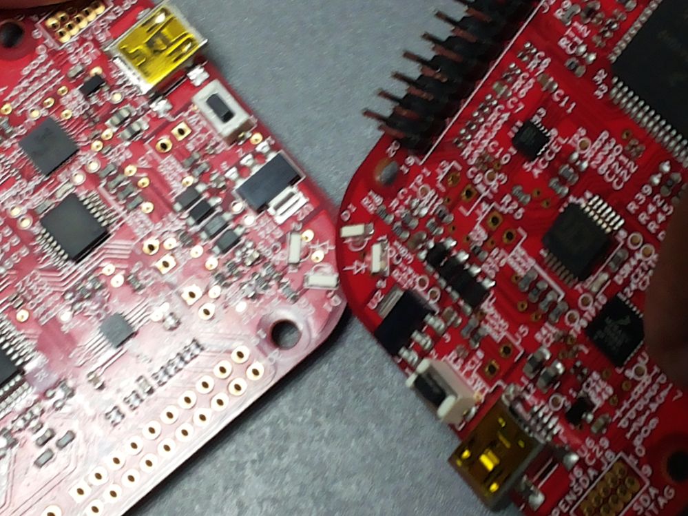
To run a single board demo, the orientation of IRDA Transmitter and IRDA receiver is already taken care as both are on the same board. But, to run the second demo, the orientation is supposed to be something like this.
Both the demos are configured for 9600baud to communicate with PC. And the IRDA communication is at 2400baud.
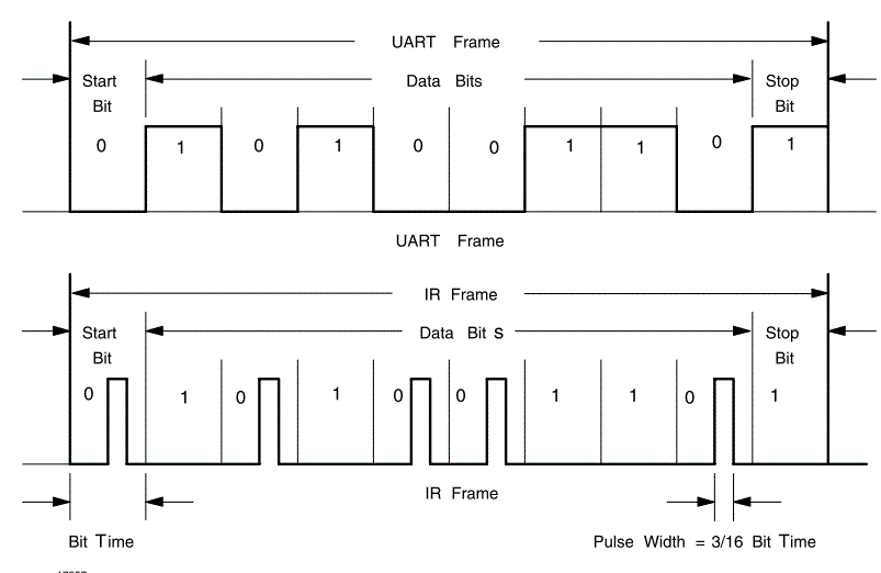
The figure in page 13 of this document is referred while development. http://www.vishay.com/docs/82513/physical.pdf
Transmission -
1. The bit width is calculated depending on the required IRDA baud and PIT1 modulo is adjusted accordingly. There are 3 MOD values initialized one after the other to generate required IR frame.
2. The data to be transmitted is sent over the HyperTerminal @ 9600baud. This data is accordingly transmitted on PTB1.
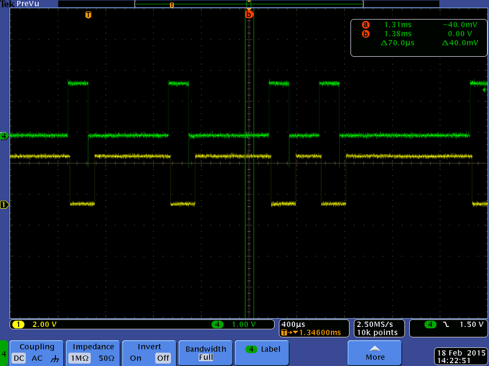
The green waveform in the below oscilloscope snap is the IR frame from the above picture. The data being sent is 'e', the hex value of which is 0x65 which can be made out from the waveform. 0x65 is 0xa6 in reverse since LSB is sent out first in the IRDA protocol[The first logic high is the start bit. In IRDA transmission, logic low is data '1' and logic high is data '0'].
Reception -
1. ACMP0 is configured to generate interrupts on either the rising edge or the falling edge.
2. The falling edge of the start bit triggers ACMP.
3. The logic received on PTA1 is decoded to arrive at the received data.
4. The falling edge on ACMP channel decides logic 0 and the PIT0 interrupt decides the logic 1.
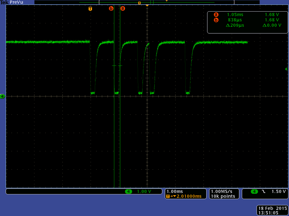
The below waveform is the one probed at PTA1.
Thanks,
Pramod TM
