- Forums
- Product Forums
- General Purpose MicrocontrollersGeneral Purpose Microcontrollers
- i.MX Forumsi.MX Forums
- QorIQ Processing PlatformsQorIQ Processing Platforms
- Identification and SecurityIdentification and Security
- Power ManagementPower Management
- Wireless ConnectivityWireless Connectivity
- RFID / NFCRFID / NFC
- Advanced AnalogAdvanced Analog
- MCX Microcontrollers
- S32G
- S32K
- S32V
- MPC5xxx
- Other NXP Products
- S12 / MagniV Microcontrollers
- Powertrain and Electrification Analog Drivers
- Sensors
- Vybrid Processors
- Digital Signal Controllers
- 8-bit Microcontrollers
- ColdFire/68K Microcontrollers and Processors
- PowerQUICC Processors
- OSBDM and TBDML
- S32M
- S32Z/E
-
- Solution Forums
- Software Forums
- MCUXpresso Software and ToolsMCUXpresso Software and Tools
- CodeWarriorCodeWarrior
- MQX Software SolutionsMQX Software Solutions
- Model-Based Design Toolbox (MBDT)Model-Based Design Toolbox (MBDT)
- FreeMASTER
- eIQ Machine Learning Software
- Embedded Software and Tools Clinic
- S32 SDK
- S32 Design Studio
- GUI Guider
- Zephyr Project
- Voice Technology
- Application Software Packs
- Secure Provisioning SDK (SPSDK)
- Processor Expert Software
- Generative AI & LLMs
-
- Topics
- Mobile Robotics - Drones and RoversMobile Robotics - Drones and Rovers
- NXP Training ContentNXP Training Content
- University ProgramsUniversity Programs
- Rapid IoT
- NXP Designs
- SafeAssure-Community
- OSS Security & Maintenance
- Using Our Community
-
- Cloud Lab Forums
-
- Knowledge Bases
- ARM Microcontrollers
- i.MX Processors
- Identification and Security
- Model-Based Design Toolbox (MBDT)
- QorIQ Processing Platforms
- S32 Automotive Processing Platform
- Wireless Connectivity
- CodeWarrior
- MCUXpresso Suite of Software and Tools
- MQX Software Solutions
- RFID / NFC
- Advanced Analog
-
- NXP Tech Blogs
- Home
- :
- MCUXpresso Software and Tools
- :
- LPCXpresso IDE FAQs
- :
- User loadable flash drivers
User loadable flash drivers
- Subscribe to RSS Feed
- Mark Topic as New
- Mark Topic as Read
- Float this Topic for Current User
- Bookmark
- Subscribe
- Mute
- Printer Friendly Page
User loadable flash drivers
- Mark as New
- Bookmark
- Subscribe
- Mute
- Subscribe to RSS Feed
- Permalink
- Report Inappropriate Content
NOTE : This FAQ refers to the flash driver interface used by LPCXpresso IDE v7.5.0 and earlier.
LPCXpresso IDE is distributed with various examples of user loadable flash drivers, for a variety of devices. However if you are using a flash device that is unsupported, it is possible to write your own driver file or adapt an existing example. This FAQ describes the process for doing so.
Please make note of any information presented with italics throughout this document.
The debug utilities for none cortex M parts have built-in flash driver support do not also support loadable flash drivers.
The Flash Driver API
The Flash API is a standard interface used by LPCXpresso debug utilities. If you supply a driver file for your debug session, the debug utility will attempt to use it for in-application flash programming. The Flash API is prototyped as follows:
// Initialize Flash Function
//////////////////////////////////////////////////////////////////////////
// Initialize Flash Programming Functions
// Parameter: adr: Device Base Address
// clk: Clock Frequency (Hz)
// fnc: Function Code (1 - Erase, 2 - Program, 3 - Verify)
// Return Value: 0 - OK, 1 - Failed
//////////////////////////////////////////////////////////////////////////
int Init (unsigned long adr, unsigned long clk, unsigned long fnc);
// De-initialize Flash Function
//////////////////////////////////////////////////////////////////////////
// De-Initialize Flash Programming Functions
// Parameter: fnc: Function Code (1 - Erase, 2 - Program, 3 - Verify)
// Return Value: 0 - OK, 1 - Failed
//////////////////////////////////////////////////////////////////////////
int UnInit (unsigned long fnc);
// Erase Sector Function
//////////////////////////////////////////////////////////////////////////
// Erase Sector in Flash Memory
// Parameter: adr: Sector Address
// Return Value: 0 - OK, 1 - Failed
//////////////////////////////////////////////////////////////////////////
int EraseSector (unsigned long adr);
// Program Page Function
//////////////////////////////////////////////////////////////////////////
// Program Page in Flash Memory
// Parameter: adr: Page Start Address
// sz: Page Size
// buf: Page Data
// Return Value: 0 - OK, 1 - Failed
//////////////////////////////////////////////////////////////////////////
int ProgramPage (unsigned long adr, unsigned long sz, unsigned char *buf);
// Blank Check Function (optional)
//////////////////////////////////////////////////////////////////////////
// Blank Check Flash Memory
// Parameter: adr: Block start address
// sz: Block size in bytes
// pat: Pattern to compare
// Return Value: 0 - when the block content is equal to the pattern pat
// 1 - when the block content differs from the pattern pat
//////////////////////////////////////////////////////////////////////////
int BlankCheck (unsigned long adr, unsigned long sz, unsigned char pat);
// Erase Complete Device Function (optional)
//////////////////////////////////////////////////////////////////////////
// Erase complete Flash Memory
// Return Value: 0 – OK
// 1 - Failed
//////////////////////////////////////////////////////////////////////////
int EraseChip (void);
// Verify Function (optional)
//////////////////////////////////////////////////////////////////////////
// Verify contents of Flash Memory with the program code
// Parameter: adr: Start address
// sz: Size in bytes
// buf: Data
// Return Value: 0 – OK
// 1 - Failed
//////////////////////////////////////////////////////////////////////////
unsigned long Verify(unsigned long adr, unsigned long sz, unsigned char *buf);
The Flash API can implement the required flash algorithm directly, or, serve as a wrapper around a vendor-supplied API. A device vendor may document the flash device algorithms, regardless of whether they supply a library in binary or source code. Most algorithms implement flash erase/program as mapped register operations, with one or more registers available to poll for completion. If you leverage a vendor supplied library (or source), it’s helpful tomap the error returns from the vendor supplied API through the wrapper in order to recognize the origin of the error.
The FlashDevice Structure
In addition to the Flash API implementation itself, the flash device configuration is specified in the FlashDevice data (FlashDev.c) declared in the struct FlashDevice structure (crt_flash_if.h). The layout of the FlashDevice data is as follows:
struct FlashSectors {
unsigned long szSector; // Sector Size in Bytes
unsigned long AddrSector; // Address of Sector
};
#define SECTOR_END 0xFFFFFFFF, 0xFFFFFFFF
struct FlashDevice {
unsigned short Vers; // Version Number and Architecture
char DevName[128]; // Device Name and Description
unsigned short DevType; // Device Type: ONCHIP, EXT8BIT, EXT16BIT, ...
unsigned long DevAdr; // Default Device Start Address
unsigned long szDev; // Total Size of Device
unsigned long szPage; // Programming Page Size
unsigned long Res; // Reserved for future Extension
unsigned char valEmpty; // Content of Erased Memory
unsigned long toProg; // Time Out of Program Page Function
unsigned long toErase; // Time Out of Erase Sector Function
struct FlashSectors *sectors;
};
Here’s a brief description how to use each of the FlashDevice fields in your device configuration. An example definition for an S25FL032 flash device follows. Vers - FLASH_DRV_VERS DevName– Device Name
- Unique string describing the device, build date and time
DevType- Device Type
- Specify one of the following:
#define UNKNOWN 0 // Unknown
#define ONCHIP 1 // On-chip Flash Memory
#define EXT8BIT 2 // External Flash Device on 8-bit Bus
#define EXT16BIT 3 // External Flash Device on 16-bit Bus
#define EXT32BIT 4 // External Flash Device on 32-bit Bus
#define EXTSPI 5 // External Flash Device on SPI
DevAdr- Device Starting Address in Code/Data space szDev - Total size of the flash device (in bytes) szPage - Programming page size szPage is the largest buffer the ProgramPage function is prepared to process each call. valEmpty - Content of Erased Memory (typically 0xFF) toProg- Timeout (in milliseconds) of ProgramPage Function
- This is the maximum time the host should wait for a program page operation to complete. Account for device program page latency, and host poll time. Note the host polls for completion of the current flash operation every 10 ms until the timeout period has expired, so select a timeout value larger than worst case.
toErase- Timeout (in milliseconds) of the EraseSector Function
- This is the maximum time the host should wait for one erase sector operation to complete. Account for largest device erase sector latency, and host poll time. Note the host polls for completion of the current flash operation every 10 ms until the timeout period has expired, so always select a timeout value larger than worst case.
sectors- Sector Configuration Array
- szSector - Sector Size in bytes
- AddrSector - Start address of sector group (as an offset from start of flash)
- Use as many entries as required to describe the sector size and start address configurations. Some devices offer sequential groups of sectors in various sizes. Each transition requires a separate FlashSectors entry. Note the AddrSector entries represent the sector address as offset from the start of flash. Therefore, the first entry is typically at sector address 0,or start of flash.
Example FlashDevice configuration for a S25FL032 flash device
The S25FL032 is a 4 MB SPIFI flash device, and is used on the NGX LPC4330/LPC1830 Explorer boards.
struct FlashDevice const FlashDevice = {
FLASH_DRV_VERS, // Driver Version, do not modify!
"LPC18/43 4MB(64KB) SPIFI @0x14000000 ("__DATE__" "__TIME__")",
EXTSPI, // Device Type
// SPIFI flash is visible in the memory map at both 0x80000000
// and 0x14000000. However 0x80000000 lies outside the code memory
// of __Cortex__-M3/M4, so we must use 0x14000000.
0x14000000, // Device Start Address
64 * 64 * 1024, // Device Size is 4MB
4096, // PROG_SIZE - Programming Page Size
0, // Reserved, must be 0
0xFF, // Initial Content of Erased Memory
500, // Program Page Timeout
5000, // Erase Sector Timeout
// Specify Size and Address of Sectors
{{64*1024, 0}, // Default sectors are 64 KB
{SECTOR_END}}
};
How the LPCXpresso IDE host uses the target-resident Flash API
When a debug session is launched, the LPCXpresso IDE loads the flash driver file, and parses the driver data for information which describes the flash device, and how the flash driver is intended to be used. The MCU interrupt state is disabled, and all active and pended interrupts are cleared. The RAM memory spanned by the flash driver block (i.e. code, data, stack, and cache) is saved internally, and the driver block is written to the target load address.
The first three calls from the host-side are made to the flash driver Init code. It's called three times successively, one each for erase/program/verify. The separate calls support unique setup for each operation, but it's unlikely a driver needs to be written this way unless under rare circumstances. These calls add significant overhead (slower operation), so are not called before each erase/program/verify call. Initialization may include setting up an external memory controller, configuring address/data lines and/or chip selects, and configuring the core clock/PLL frequency for flash operations. The LPCXpresso IDE host-side is not guaranteed to provide a valid clock frequency to an Init call, so it’s safer to complete all clock/PLL setup in this code.
Chip erase uses either the EraseChip API call (if implemented), or the EraseSector API call. The EraseSector call is used for each sector in flash. One reason to provide only an EraseSectorAPI is the case where flash will be programmed with separate images at different times. This allows you to preserve the flash content from previous programming operations.
A host-side flash program sequence is typically BlankCheck -> EraseSector (erase by sector) -> ProgramPage -> Verify. There may be one or more pages within a sector. For those pages not on a sector boundary, the sequence is ProgramPage -> Verify. If the Verify API call is not implemented, the debug utility will verify flash contents against its image buffer. This is recommended, since it typically results in faster driver operation. Otherwise, the debug utility uses a subsequent Verify call to the target-resident driver after each ProgramPage.
At the end of the erase/ program sequences, the last three calls are made to the flash driver UnInitcode. It's called three times successively to handle erase/program/verify setup restore, if required. It’s rarely necessary to implement this call. These calls can add significant overhead (slow operation), so are not called after each erase/program/verify call. Finally, the flash driver block is unloaded by restoring the RAM contents overwritten by the flash driver block, and the processor is typically reset.
It is desirable to specify the largest page size possible in the device structure, with an optimum size being ~4 KB. Available target SRAM may dictate a page size limit less than optimal, since the target-resident flash driver code/data/stack shares available space. The page size used by the LPCXpresso IDE host-side is considered the largest buffer a ProgramPage operation can support. This size is typically a multiple of (or evenly divisible by) the device page size provided the actual device details are handled in the flash driver. A future optimization may combine at least the program and verify operations in one call.
A zero return from the flash driver API signifies success, non-zero signifies failure. All non-zero error returns by the Flash API are considered fatal. Error codes can be more descriptive than 0 or 1 if a different non-zero return helps to identify the failure (e.g. an error return from a vendor supplied library).API errors are formatted and displayed as:
"Ec: Flash driver \"%s\" return code: 0x%X", op, errorcode
Where ‘op’ is one of Init, ProgramPage, EraseSector, EraseChip, BlankCheck, Verify, UnInit, or Unknown, and ‘errorcode’ is the actual 32-bit return code from the API method.
If an API call does not return, the host-side will eventually time out waiting for completion. The timeout is dependent on the value(s) supplied in the FlashDevice data structure for erase/program. If a timeout occurs in an operation other than erase/program, the timeout used is 1500 milliseconds (1.5 seconds). A timeout error is formatted as:
"Ec: Flash driver \"%s\" timeout (%d ms) PC: %08X\n", op, timeout, PC
Where ‘timeout’ is represented in milliseconds, and ‘PC’ is the program counter in effect when the host-side timeout occurred. This may help to identify problems in the Flash API, or a fault condition.
What is the difference between a sector and a page?
A flash sector is the smallest amount of flash memory that can be erased in one pass.
A flash page is the smallest amount of flash memory that can be programmed in one pass.
Typically a flash sector will consist of a number of flash pages, but the size of both pages and sectors is vendor/part specific. Thus you will need to check the vendor documentation or with the vendor for the flash device(s) you are using.
It is important to reiterate the distinction between a device page size, and the exported (or advertised) page size specified in the FlashDevice 'szPage' entry (FlashDev.c). The exported page size is used by the host-side as the maximum size image buffer the host can safely send per call to the target-resident ProgramPage API. The ProgramPage implementation must accommodate any restrictions imposed by a fixed size device page, and be prepared to handle partial buffers. The exported page size is directly related to flash program time.
Flash Driver Projects
Your flash driver project as a minimum should include 6 source/header files. These are
- crt_flash_if.c – MemoryDevice_t data definition (do not edit)
- crt_flash_if.h – struct FlashDevice, MemoryDevice_t, and Flash API declarations (do not edit)
- FlashPrg.c – Flash API implementation
- FlashDev.c – struct FlashDevice data definition(s).
- main.c – RAM resident test harness used to exercise the Flash API. A test harness can typically use the linker scripts created by the Code Red IDE Wizard.>
- cr_startup_xx.c – Part-specific startup code included for use with the test harness (e.g. cr_startup_lpc18xx.c, cr_startup_lpc178x.c, etc.). In the standalone flash driver build, the Init Flash API may need to duplicate part of the standard startup sequence.
The flash driver project may include multiple configurations. As a minimum, you’ll need a Debug configuration for the test harness, and separate configurations for each flash device. If multiple flash configurations are supported, you can use conditional compilation directives where appropriate in FlashDev.c and FlashPrg.c for each project configuration.
Do not rely on zero initial values in variables allocated to any .bss section unless you’ve added your own code to zero initialize this section (e.g. Init). Most driver implementations do not require extensive global data sets, so standard practice should be to provide an initial value (or zero) at declaration.
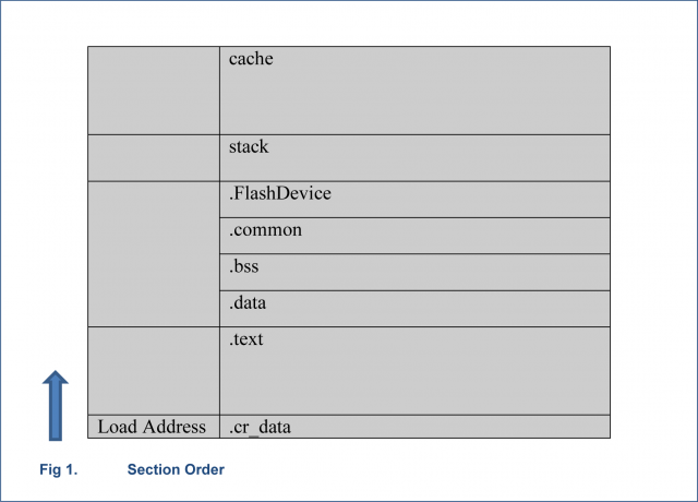
A custom linker script, FlashDriver.ld, is used for the final driver image. An example script is provided in the SPIFI flash driver example project. It’s critical the FlashDriver.ld section order be maintained in the link for the final driver image. Be certain to exclude code/data contributed from the test harness configuration. If your driver implementation creates custom named sections, the section order must not supersede the FlashDriver.ld section order. The final driver image should be ordered as follows, from the RAM Load address:
Figure 1 - Section Order
Flash driver files ready for deployment testing, or deployment should be named with a .cfx file extension, and placed in the Flash subdirectory in the LPCXpresso IDE installation (see below). There are two configuration parameters in the FlashDriver.ld linker script which reserve space for the flash driver stack, and image cache you may need to modify. These are:
__stack_size = 1024;          /* stack size */
__cache_size = 4096;          /* flash image buffer size */
The __stack_size to reserve depends on the stack requirements of your driver implementation. It must accommodate all local data defined within each method in the Flash API, the thread of execution, and on any recursion in the driver itself. If your Flash API wraps around a vendor API supplied only in binary form, you may need to consult with the vendor on stack requirements. The __cache_size to reserve should be equal to the FlashDevice szPage entry. The interrelationship between page size, cache size, and sector size may not be readily apparent in your driver implementation.
Testing the Flash Driver
Building a test harness
An example test harness (main.c) is supplied in the SPIFI example project, and should be modified for your use. The purpose of the test harness is to validate the operation of each method exported by the Flash API. The Init function configures your hardware to erase/program your flash device. Be certain the setup configures your hardware as intended (memory controller, address/data lines, clock/PLL, etc.). The ProgramPage function is usually tested by a writing a repeating pattern to flash, and verifying the flash memory against the pattern. The EraseSector method receives an absolute address of a sector bound. Be certain it translates the sector address to the represented sector, and completely erases the sector. The contents of the sector should show valEmpty content for each byte in the sector. Note the test harness example does not make use of the FlashDevice toProg and toErase timeout values. Use the vendor documentation, and your test harness observations to make adjustments to the exported timeout values. The UnInitcode is often unimplemented. The host-side will at least reset the core after flash program, so it’s usually not needed.
Deployment
Once the flash driver passes the basic test harness validation, the remaining tests are done as a deployed driver. As noted above, once a deployable .cfx file has been generated, it should be placed with the other drivers in the Flash subdirectory of the LPCXpresso IDE installation prior to use. The Flash folder location depends on the particular LPCXpresso IDE installation but will be of the form:
C:\nxp\LPCXpresso_<ver>_<build>\lpcxpresso\bin\Flash
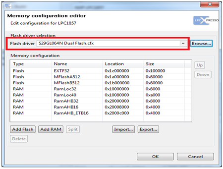
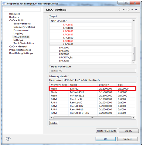
Once the .cfx file has been added, the project to be flashed needs to be modified in order to use the new flash driver file. First, the new memory configuration (External Flash) needs to be added to the MCU selected. This can be done by selecting the C/C++ Build->MCU settings (in the Project Properties window) and clicking Edit and adding the memory as shown in Figure 2. Note the Location and Size columns in the Memory configuration editor should match the exported FlashDevice DevAdr and szDev fields.
Fig 2. Memory configuration editor
The same dialog box (shown in Figure 2) can be used to add the name of the flash driver file (e.g. S29GL064N_Dual_Flash.cfx). The window appears as shown above.
Fig 3. Region
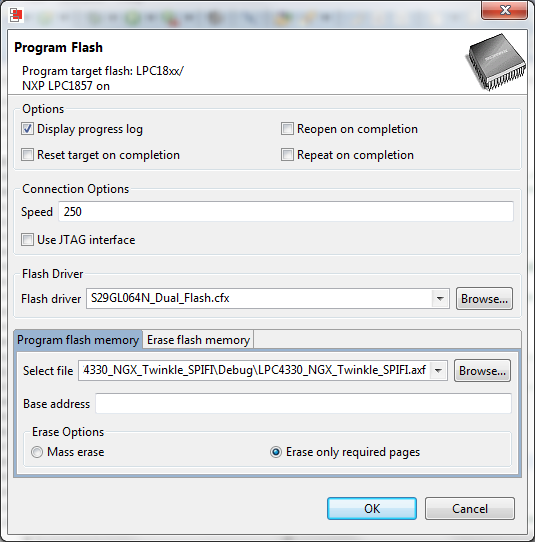
Once these changes are complete, a sample application should be built to locate in the added memory region. The binary file is programmed into the Flash memory by clicking on the Program Flash button, shown in Figure 3, and selecting the corresponding .axf file, as shown in Figure 4. This will program the flash memory using your new flash device. The board needs to be reset after this.
Fig 4. Program Flash Icon
Fig 5. Flash Dialog
As a debug aid, you can check the “Display progress log” box to view the console output from the erase/program operation. The debug utility can be also
used standalone from the command-line (DOS command window). An example command-line will be displayed in the progress log. You should navigate to
the LPCXpresso bin directory to use a debug utility from the command-line:
C:\nxp\LPCXpresso_<ver>_<build>\lpcxpresso\bin\
If you set the CRT_DEBUG_TRACE=1 environment variable prior to using a command-line flash operation, additional register context is output to the console
upon error. This includes core register state, bus fault status, etc..


