- Forums
- Product Forums
- General Purpose MicrocontrollersGeneral Purpose Microcontrollers
- i.MX Forumsi.MX Forums
- QorIQ Processing PlatformsQorIQ Processing Platforms
- Identification and SecurityIdentification and Security
- Power ManagementPower Management
- Wireless ConnectivityWireless Connectivity
- RFID / NFCRFID / NFC
- Advanced AnalogAdvanced Analog
- MCX Microcontrollers
- S32G
- S32K
- S32V
- MPC5xxx
- Other NXP Products
- S12 / MagniV Microcontrollers
- Powertrain and Electrification Analog Drivers
- Sensors
- Vybrid Processors
- Digital Signal Controllers
- 8-bit Microcontrollers
- ColdFire/68K Microcontrollers and Processors
- PowerQUICC Processors
- OSBDM and TBDML
- S32M
- S32Z/E
-
- Solution Forums
- Software Forums
- MCUXpresso Software and ToolsMCUXpresso Software and Tools
- CodeWarriorCodeWarrior
- MQX Software SolutionsMQX Software Solutions
- Model-Based Design Toolbox (MBDT)Model-Based Design Toolbox (MBDT)
- FreeMASTER
- eIQ Machine Learning Software
- Embedded Software and Tools Clinic
- S32 SDK
- S32 Design Studio
- GUI Guider
- Zephyr Project
- Voice Technology
- Application Software Packs
- Secure Provisioning SDK (SPSDK)
- Processor Expert Software
- Generative AI & LLMs
-
- Topics
- Mobile Robotics - Drones and RoversMobile Robotics - Drones and Rovers
- NXP Training ContentNXP Training Content
- University ProgramsUniversity Programs
- Rapid IoT
- NXP Designs
- SafeAssure-Community
- OSS Security & Maintenance
- Using Our Community
-
- Cloud Lab Forums
-
- Knowledge Bases
- ARM Microcontrollers
- i.MX Processors
- Identification and Security
- Model-Based Design Toolbox (MBDT)
- QorIQ Processing Platforms
- S32 Automotive Processing Platform
- Wireless Connectivity
- CodeWarrior
- MCUXpresso Suite of Software and Tools
- MQX Software Solutions
- RFID / NFC
- Advanced Analog
-
- NXP Tech Blogs
- Home
- :
- General Purpose Microcontrollers
- :
- Kinetis Microcontrollers
- :
- I2S interface
I2S interface
- Subscribe to RSS Feed
- Mark Topic as New
- Mark Topic as Read
- Float this Topic for Current User
- Bookmark
- Subscribe
- Mute
- Printer Friendly Page
I2S interface
- Mark as New
- Bookmark
- Subscribe
- Mute
- Subscribe to RSS Feed
- Permalink
- Report Inappropriate Content
Hi everyone,
I am trying to interface an ADC to K60 MCU (TWR-K60F512) using I2S interface.
ADC is always a MASTER
Reading ADC:
Please see the below timing diagram of ADC, which shows how it transmits the conversion results.
Following are the ADC signals related to ADC Read :
a) Serial Clock Output (SCO),
b) Frame Synchronization Output (FSO)
c) Serial Data Output (SDO)
- The data read from ADC is clocked out using Serial Clock Output(SCO).
- The conversion result output on the SDO line is framed by the frame synchronization output FSO, which is sent logic low for 32 SCO cycles.
- Each bit of the new conversion result is clocked onto SDO line on the rising SCO edge and is valid on the falling SCO edge.
- The 32-bit result consists of 24 data bits followed by 8 status bits.
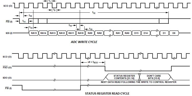
Writing ADC:
Please see the below timing diagram of ADC which shows how a write operation is performed.
Following are the ADC signals related to ADC write:
a) Serial Clock Output (SCO) same as above
b) Frame Synchronization Input (FSI)
c) Serial Data Input (SDI)
- Serial writing operation is synchronous to SCO signal.
- The status of the FSI is checked on the falling edge of the SCO signal. If FSI line is low, then first data bit on the SDI line is latched on the next SCO falling edge.
- FSI signal is made low at a position when SCO signal is high or low to allow setup and hold times from the SCO falling edge to be met.
- The width of the FSI signal can be set to between 1 and 32 SCO periods wide.
- Write data is pumped onto SDI with sync to SCO.
- A second or subsequent falling edge that occurs before 32 SCO periods have elapsed is ignored.
For this requirement, I planned to interface ADC to I2S module as follows:
SCO -> I2S0_RX_BCLK, I2S_TX_BCLK
FSO -> I2S0_RX_FS
SDO -> I2S0_RX_D0
FSI <- I2S0_TX_FS
SDI <- I2S0_TX_D0
Please review the configuration and suggest the required configuration settings like Mode (Synchronous, Asynchronous, Synchronous with Other SAI..) and other configuration register settings.
Thanks in advance
Gourah
- Mark as New
- Bookmark
- Subscribe
- Mute
- Subscribe to RSS Feed
- Permalink
- Report Inappropriate Content
Can anyone there, please respond, awaiting your replies.
Thanks
- Mark as New
- Bookmark
- Subscribe
- Mute
- Subscribe to RSS Feed
- Permalink
- Report Inappropriate Content
Hello Gourah,
Sorry for late response but i needed to confirm some details.
I reviewed your configuration and this could not be achieved using K60's SAI module.
For reception (ADC's reading cycles), SAI module will work with no problem.
Problem here is Transmission (writing cycle), it is not possible to synchronize Frame Sync signal to bit clock. SAI module supports 2 cases: Configured as Master in which all clocks are generated by SAI or Configured as Slave in which SAI module receives clocks from Master. In your case, Bit clock will be generated in ADC chip and Frame Sync In needs to be generated by SAI, so this configuration is not supported.
You can use a newer K6x part that contains FlexIO module, in which, you can emulate this SAI functionality without problems on synchronizing Frame Sync and Bit clock signals.
I hope this can help you.
Best Regards,
Isaac

