- Forums
- Product Forums
- General Purpose MicrocontrollersGeneral Purpose Microcontrollers
- i.MX Forumsi.MX Forums
- QorIQ Processing PlatformsQorIQ Processing Platforms
- Identification and SecurityIdentification and Security
- Power ManagementPower Management
- Wireless ConnectivityWireless Connectivity
- RFID / NFCRFID / NFC
- Advanced AnalogAdvanced Analog
- MCX Microcontrollers
- S32G
- S32K
- S32V
- MPC5xxx
- Other NXP Products
- S12 / MagniV Microcontrollers
- Powertrain and Electrification Analog Drivers
- Sensors
- Vybrid Processors
- Digital Signal Controllers
- 8-bit Microcontrollers
- ColdFire/68K Microcontrollers and Processors
- PowerQUICC Processors
- OSBDM and TBDML
- S32M
- S32Z/E
-
- Solution Forums
- Software Forums
- MCUXpresso Software and ToolsMCUXpresso Software and Tools
- CodeWarriorCodeWarrior
- MQX Software SolutionsMQX Software Solutions
- Model-Based Design Toolbox (MBDT)Model-Based Design Toolbox (MBDT)
- FreeMASTER
- eIQ Machine Learning Software
- Embedded Software and Tools Clinic
- S32 SDK
- S32 Design Studio
- GUI Guider
- Zephyr Project
- Voice Technology
- Application Software Packs
- Secure Provisioning SDK (SPSDK)
- Processor Expert Software
- Generative AI & LLMs
-
- Topics
- Mobile Robotics - Drones and RoversMobile Robotics - Drones and Rovers
- NXP Training ContentNXP Training Content
- University ProgramsUniversity Programs
- Rapid IoT
- NXP Designs
- SafeAssure-Community
- OSS Security & Maintenance
- Using Our Community
-
- Cloud Lab Forums
-
- Knowledge Bases
- ARM Microcontrollers
- i.MX Processors
- Identification and Security
- Model-Based Design Toolbox (MBDT)
- QorIQ Processing Platforms
- S32 Automotive Processing Platform
- Wireless Connectivity
- CodeWarrior
- MCUXpresso Suite of Software and Tools
- MQX Software Solutions
- RFID / NFC
- Advanced Analog
-
- NXP Tech Blogs
- Home
- :
- General Purpose Microcontrollers
- :
- Kinetis Microcontrollers
- :
- 12 bit DAC in k40 Series
12 bit DAC in k40 Series
- Subscribe to RSS Feed
- Mark Topic as New
- Mark Topic as Read
- Float this Topic for Current User
- Bookmark
- Subscribe
- Mute
- Printer Friendly Page
- Mark as New
- Bookmark
- Subscribe
- Mute
- Subscribe to RSS Feed
- Permalink
- Report Inappropriate Content
Hi
I'm using the DAC in "non buffer" mode, SW trigger
1. What is the SW trigger for the DAC to start convert form digital to analog? Is it the write to DATA registers ? (high register or low register ?)
2. What bit tell me that the conversion is completed, and I can convert new data?
3. If I configure the two DAC's in my MCU (DAC0, DAC1) to start convert, is the data converted in parallel?
Thanks
Solved! Go to Solution.
- Mark as New
- Bookmark
- Subscribe
- Mute
- Subscribe to RSS Feed
- Permalink
- Report Inappropriate Content
Hi
1. When the SW mode is selcted (DACTRGSET set) a write to DAT0 triggers the conversion. The Freescale examples write DATL followed by DATH but I found that a single half-word write has the same effect and is of course more efficient.
2. There is no status bit showing the status of the conversion. The delay between triggering the new value and the output settling to its final value depends on the size of the voltage change and also whether the low power or high power operation is set - the high power mode is about 7x faster. Since the output change is a "settling time" rather than a conversion as such (a bit like charging a capacitor to the new value) the speed of writing should be done in accordance to the worst case settling charge - if faster, it will result in a low-pass filter action since the output can't get to the intermediate value. Triggering from a timer is probably the best method if writing continually at a fast rate - it is also important to have an accurate base clock in case of generating specific waveforms.
3. DAC0 and DAC1 are independent and so work in parallel.
Regards
Mark
- Mark as New
- Bookmark
- Subscribe
- Mute
- Subscribe to RSS Feed
- Permalink
- Report Inappropriate Content
Hi mf_kappa,
Because this post is a few years old i'm not sure if i should be asking this question here.
Basically for the past month I've been learning embedded programming while working with TWR-K40X256 (MK40DX256ZVMD10 micro-controller). Right now I'm tasked with converting a generic sinusoidal wave (like a sum of sines) via ADC, applying some basic digital signal processing to the data and then converting the processed digital data back to analog using DAC (kinda similar to yours if i understood correctly).
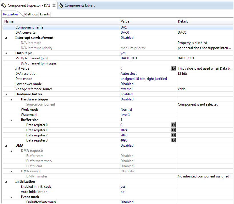
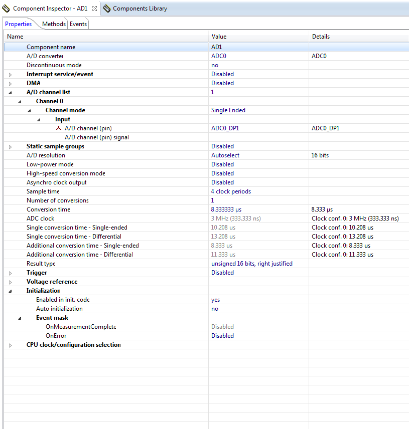
I've decided to use Processor Expert for this and so I've added the components DAC_LDD and ADC_LDD to the project (images of the configurations below).
Looking through the Typical Usage for both the components I've tried to implement a continuous measurement of a selected sample group (w/ interrupt service) without much success (measured values are always 0) and for the DAC part i am generally not sure about the way to implement the conversion.
Do you have some suggestions or code snippets on how to solve the problem/implement the system I explained?
I'm sure this is a basic work and all these doubts must be born on my inexperience.
Thank you for all the attention!
- Mark as New
- Bookmark
- Subscribe
- Mute
- Subscribe to RSS Feed
- Permalink
- Report Inappropriate Content
Hi Francisco
I can't help with the PE setup but if you want a working solution you can simply use the uTaskerV1.4 project which includes a buffered ADC/DAC configuration based on DMA and PDB which is very practical for adding signal processing in between.
The ADC/DAC configuration and operatrion is explained in the document http://www.utasker.com/docs/uTasker/uTaskerADC.pdf
Download the uTasker project from http://www.utasker.com/forum/index.php?topic=1721.0 - it will build with CW, KDS, IAR, Keil, Rowley, Atollic, Coo Cox, standalone GCC or Visual Studio. Then select your processor and board in config.h:
#define KINETIS_K40 // choose family
#define TWR_K40X256 // choose board
In app_hw_kinetis.h enable both ADC and DAC support: #define SUPPORT_ADC and #define SUPPORT_DAC
In ADC_Timers.h enable the ADC/DAC operation with #define TEST_AD_DA and make any configuration changes according to the interfaces in the document (sampling rate, resolution, buffer size, DMA channel allocation etc.)
On each half-buffer completion there is an event ADC_TRIGGER_1 (see handling in ADC_Timers.h) and code there can process the buffer as required - it has to be complete before the next half buffer is required so adjusting the buffer size allows compromising between buffer processing rate and delay.
Regards
Mark
- Mark as New
- Bookmark
- Subscribe
- Mute
- Subscribe to RSS Feed
- Permalink
- Report Inappropriate Content
Hi
As reference I have built the project for the K40 tower board (with settings as above) and attached it as binary file. The potentiometer voltage (on ADC input ADC_DM1_SINGLE) is passed to the DAC0 output (A32 on the primary back plane connector) after a 1s delay.
In addition it will drive the SLCD module with the time (RTC) and there is a command line menu on the serial connector (115200Baud).
Regards
Mark
- Mark as New
- Bookmark
- Subscribe
- Mute
- Subscribe to RSS Feed
- Permalink
- Report Inappropriate Content
Hi
1. When the SW mode is selcted (DACTRGSET set) a write to DAT0 triggers the conversion. The Freescale examples write DATL followed by DATH but I found that a single half-word write has the same effect and is of course more efficient.
2. There is no status bit showing the status of the conversion. The delay between triggering the new value and the output settling to its final value depends on the size of the voltage change and also whether the low power or high power operation is set - the high power mode is about 7x faster. Since the output change is a "settling time" rather than a conversion as such (a bit like charging a capacitor to the new value) the speed of writing should be done in accordance to the worst case settling charge - if faster, it will result in a low-pass filter action since the output can't get to the intermediate value. Triggering from a timer is probably the best method if writing continually at a fast rate - it is also important to have an accurate base clock in case of generating specific waveforms.
3. DAC0 and DAC1 are independent and so work in parallel.
Regards
Mark
- Mark as New
- Bookmark
- Subscribe
- Mute
- Subscribe to RSS Feed
- Permalink
- Report Inappropriate Content
Hi Mark
Thanks for your answer !
I still have a question regards the DAC:
You recomended to trigger the DAC from a timer. In my application, I need to wait a ADC conversion
before triggering the DAC. (The basic flow of this application is: sampling data via ADC, then perform math operations of the digital sampling, Finally, convert the digital data to analog using DAC)
My application need to work very fast rate.
Do you reccomend to trigger the ADC and the DAC using the same timer?
Or trigger only the ADC by timer and trigger the DAC by SW (wait until ADC finish sampling)?
Regards
- Mark as New
- Bookmark
- Subscribe
- Mute
- Subscribe to RSS Feed
- Permalink
- Report Inappropriate Content
Hi
That is a design question which may have several different possible answers.
Since I haven't used the buffered mode (yet) I don't know all details but I known that the timer modules can be used to tigger DAC conversions (with up to15 buffered output values in a queue). DMA is possible and it is also possible to trigger the DAC from the ADC.
Since you need to process the ADC value before sending it to the DAC it may be interesting to use the buffer as short delay line - ADC and DAC triggered essentially from the same timer but the buffers used to allow some jitter in the SW time from the ADC inputs to the DAC outputs. As long as the buffer doesn't completely empty the SW just has to ensure that there is at least one sample ready when needed. Whether you can affort a few samples of delay depends on the exact requirements but it may be better than having jitter on the exact output sample time due to SW jitter between the ADC input sample completion and the DAC write.
Regards
Mark
- Mark as New
- Bookmark
- Subscribe
- Mute
- Subscribe to RSS Feed
- Permalink
- Report Inappropriate Content
Hi Mark
Thanks you very much for your answers, again !

