- Forums
- Product Forums
- General Purpose MicrocontrollersGeneral Purpose Microcontrollers
- i.MX Forumsi.MX Forums
- QorIQ Processing PlatformsQorIQ Processing Platforms
- Identification and SecurityIdentification and Security
- Power ManagementPower Management
- Wireless ConnectivityWireless Connectivity
- RFID / NFCRFID / NFC
- MCX Microcontrollers
- S32G
- S32K
- S32V
- MPC5xxx
- Other NXP Products
- S12 / MagniV Microcontrollers
- Powertrain and Electrification Analog Drivers
- Sensors
- Vybrid Processors
- Digital Signal Controllers
- 8-bit Microcontrollers
- ColdFire/68K Microcontrollers and Processors
- PowerQUICC Processors
- OSBDM and TBDML
- S32M
-
- Solution Forums
- Software Forums
- MCUXpresso Software and ToolsMCUXpresso Software and Tools
- CodeWarriorCodeWarrior
- MQX Software SolutionsMQX Software Solutions
- Model-Based Design Toolbox (MBDT)Model-Based Design Toolbox (MBDT)
- FreeMASTER
- eIQ Machine Learning Software
- Embedded Software and Tools Clinic
- S32 SDK
- S32 Design Studio
- GUI Guider
- Zephyr Project
- Voice Technology
- Application Software Packs
- Secure Provisioning SDK (SPSDK)
- Processor Expert Software
-
- Topics
- Mobile Robotics - Drones and RoversMobile Robotics - Drones and Rovers
- NXP Training ContentNXP Training Content
- University ProgramsUniversity Programs
- Rapid IoT
- NXP Designs
- SafeAssure-Community
- OSS Security & Maintenance
- Using Our Community
-
- Cloud Lab Forums
-
- Knowledge Bases
- ARM Microcontrollers
- i.MX Processors
- Identification and Security
- Model-Based Design Toolbox (MBDT)
- QorIQ Processing Platforms
- S32 Automotive Processing Platform
- Wireless Connectivity
- CodeWarrior
- MCUXpresso Suite of Software and Tools
- MQX Software Solutions
-
- Home
- :
- i.MX フォーラム
- :
- i.MX RT クロスオーバーMCU
- :
- How to debug iMX.RT105x with SWD interface after programming secure JTAG eFuse
How to debug iMX.RT105x with SWD interface after programming secure JTAG eFuse
- RSS フィードを購読する
- トピックを新着としてマーク
- トピックを既読としてマーク
- このトピックを現在のユーザーにフロートします
- ブックマーク
- 購読
- ミュート
- 印刷用ページ
- 新着としてマーク
- ブックマーク
- 購読
- ミュート
- RSS フィードを購読する
- ハイライト
- 印刷
- 不適切なコンテンツを報告
Hi,
As AN12419, I have programmed the secure JTAG eFuse. Below are the details.
- Program the response key, SJC_RESP
- Program 0x1 in the eFuse JTAG_SMODE to switch the SJC to Secure JTAG mode
- Program 0x1 in the eFuse KTE_FUSE
- Program 0x1 in the eFuse SJC_RESP_LOCK to disable read/write access of the secret response key
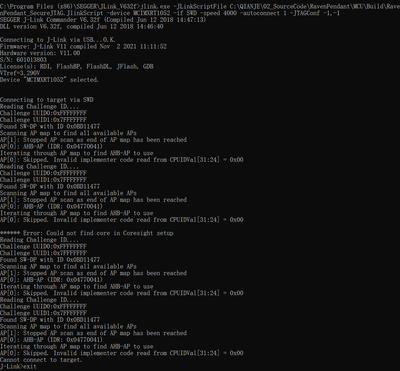
I haven't programed 0x1 in the eFuse DAP_SJC_SWD_SEL to switch the DAP to the JTAG mode. Because my board uses SWD interface. I created a file of NXP_RT1052_SecureJTAG.JlinkScript as 4.2 Example of SEGGER J-link Secure JTAG unlock script. Use the below command to connect the device. It failed to connect to the device.
jlink.exe -JLinkScriptFile NXP_RT1052_SecureJTAG.JlinkScript -device MCIMXRT1052 -if SWD -speed 4000 -autoconnect 1 -JTAGConf -1,-1
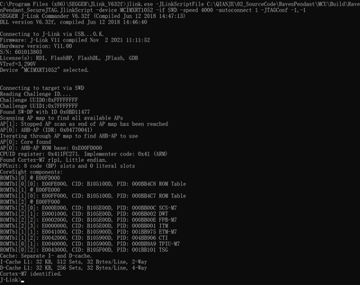
I have tried several times and found that if I send below command first. Then repeat above command, it works.
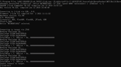
jlink.exe -JLinkScriptFile NXP_RT1052_SecureJTAG.JlinkScript -device MCIMXRT1052 -if JTAG -speed 4000 -autoconnect 1 -JTAGConf -1,-1
Do you have any suggestion (JlinkScript and command) about SWD interface?
解決済! 解決策の投稿を見る。
- 新着としてマーク
- ブックマーク
- 購読
- ミュート
- RSS フィードを購読する
- ハイライト
- 印刷
- 不適切なコンテンツを報告
Hi @JerryQian_Shure ,
Answer your questions:
Does it mean the authentication process (secure JTAG mechainsm) only supports JTAG interface?
=>Yes, so you still need to use the JTAG, I mean, you need to follow the AN to burn the JTAG interface, then use the JTAG debug instead of the SWD, as the fuse can't be back.
Does only secure JTAG interface support the authentication process?
=> Yes, yesterday our AE confirm it.
After finish the authentication, can switch to SWD interface to debug? From step 4, seems yes.
=> After you use the JTAG secure with JTAG interface, can't back to SWD. Just use the JTAG instead of the SWD. You board should use the JTAG, follow the NXP EVK JTAG interface.
Best Regards,
Kerry
- 新着としてマーク
- ブックマーク
- 購読
- ミュート
- RSS フィードを購読する
- ハイライト
- 印刷
- 不適切なコンテンツを報告
Hi @JerryQian_132 ,
To RT10XX, the default debug interface is SWD interface, if you want ot use the JTAG, you need to burn the related fuse bit from SWD to JTAG.
But, please note, fuse, just can from 0 to 1, can't be back.
So, if you already switch it to the JTAG, just use the JTAG debug, SWD can't be used anymore, and fuse can't be back.
Wish it helps you!
Best Regards,
Kerry
- 新着としてマーク
- ブックマーク
- 購読
- ミュート
- RSS フィードを購読する
- ハイライト
- 印刷
- 不適切なコンテンツを報告
Hi Kerry, I don't want to use JTAG interface. I'm using SWD interface. I haven't programmed the 0x1 in the eFuse DAP_SJC_SWD_SEL. It's still 0 to select SWD. My question is how to debug(or unlock) with SWD interface.
I found I have to send below two commands to unlock secure JTAG when use SWD interface.
- jlink.exe -JLinkScriptFile NXP_RT1052_SecureJTAG.JlinkScript -device MCIMXRT1052 -if JTAG -speed 4000 -autoconnect 1 -JTAGConf -1,-1
- jlink.exe -JLinkScriptFile NXP_RT1052_SecureJTAG.JlinkScript -device MCIMXRT1052 -if SWD -speed 4000 -autoconnect 1 -JTAGConf -1,-1
Is there any method to send one command to unlock secure JTAG (using SWD interface)?
- 新着としてマーク
- ブックマーク
- 購読
- ミュート
- RSS フィードを購読する
- ハイライト
- 印刷
- 不適切なコンテンツを報告
My understand is, the secure mode just support the JTAG, not the SWD.
Do you mean, you use your SWD command, and associated with SEGGER J-link Secure JTAG unlock script, you can unlock the chip?
Can you also share some unlock screen about it, just like the AN12419 4.1 Steps to connect J-Link debugger via Secure JTAG
Then, I will help you to check it internaly.
Best Regards,
Kerry
- 新着としてマーク
- ブックマーク
- 購読
- ミュート
- RSS フィードを購読する
- ハイライト
- 印刷
- 不適切なコンテンツを報告
My board only reserved the SWD interface. But for security requirement, I have to enable the secure JTAG. After programmed the eFuse bits, I'm investigating how to debug with SWD interface.
- Reboot the device. IAR cannot debug my code.
- Reboot the device. Send my SWD command and associated with SEGGER J-link Secure JTAG unlock script. IAR still cannot debug.
- Reboot the device. Send my JTAG command and my SWD command and associated with SEGGER J-link Secure JTAG unlock script. IAR can debug.
- Reboot the device. Send my JTAG command and associated with SEGGER J-link Secure JTAG unlock script. IAR can debug.
So, my questions are
- Does only secure JTAG interface support the authentication process?
- After finish the authentication, can switch to SWD interface to debug? From step 4, seems yes.
- 新着としてマーク
- ブックマーク
- 購読
- ミュート
- RSS フィードを購読する
- ハイライト
- 印刷
- 不適切なコンテンツを報告
Hi @JerryQian_Shure ,
Answer your questions:
Does it mean the authentication process (secure JTAG mechainsm) only supports JTAG interface?
=>Yes, so you still need to use the JTAG, I mean, you need to follow the AN to burn the JTAG interface, then use the JTAG debug instead of the SWD, as the fuse can't be back.
Does only secure JTAG interface support the authentication process?
=> Yes, yesterday our AE confirm it.
After finish the authentication, can switch to SWD interface to debug? From step 4, seems yes.
=> After you use the JTAG secure with JTAG interface, can't back to SWD. Just use the JTAG instead of the SWD. You board should use the JTAG, follow the NXP EVK JTAG interface.
Best Regards,
Kerry
- 新着としてマーク
- ブックマーク
- 購読
- ミュート
- RSS フィードを購読する
- ハイライト
- 印刷
- 不適切なコンテンツを報告
Hi Kerry,
Sure. The eFuse settings are 0x400 : 0x40128043 and 0x460 : 0x04400012.
My test script has attached. Below are my steps.
- Step 1: reboot the device
- Step 2: jlink.exe -JLinkScriptFile NXP_RT1052_SecureJTAG.JlinkScript -device MCIMXRT1052 -if SWD -speed 4000 -autoconnect 1 -JTAGConf -1,-1
Cannot connect to the target - Step 3: jlink.exe -JLinkScriptFile NXP_RT1052_SecureJTAG.JlinkScript -device MCIMXRT1052 -if JTAG -speed 4000 -autoconnect 1 -JTAGConf -1,-1
Cannot connect to the target. But can read the challenge ID - Step 4: jlink.exe -JLinkScriptFile NXP_RT1052_SecureJTAG.JlinkScript -device MCIMXRT1052 -if SWD -speed 4000 -autoconnect 1 -JTAGConf -1,-1
Cannot read the challenge ID. But can connect to the target.
Is it possible that combine step 3 and 4 with one command? Change the script?
- 新着としてマーク
- ブックマーク
- 購読
- ミュート
- RSS フィードを購読する
- ハイライト
- 印刷
- 不適切なコンテンツを報告
Hi @JerryQian_132 ,
Today, I talk your issue with our AE, and I get the information that, to the secure debug, our RT just support the secure JTAG, not support the secure SWD, so, your this type testing is no meanning.
If you want to use the secure debug interface, you still need to use the Secure JTAG, not the SWD. If you just want to debug, SWD is OK, you don't need to add the secure.
Thanks a lot for your understanding.
Wish it helps you!
Best Regards,
Kerry
- 新着としてマーク
- ブックマーク
- 購読
- ミュート
- RSS フィードを購読する
- ハイライト
- 印刷
- 不適切なコンテンツを報告
OK. Does it mean the authentication process (secure JTAG mechainsm) only supports JTAG interface? I have to finish the authentication (secret response key) with JTAG interface first. Then can debug with SWD interface?
I have tried below process. It works.
- Run "jlink.exe -JLinkScriptFile C:\QIANJE\02_SourceCode\RavenPendant\MCU\Build\RavenPendant_SecureJTAG.JlinkScript -device MCIMXRT1052 -if JTAG -speed 4000 -autoconnect 1 -JTAGConf -1,-1" to unlock the device.
- Open IAR to debug my code
- 新着としてマーク
- ブックマーク
- 購読
- ミュート
- RSS フィードを購読する
- ハイライト
- 印刷
- 不適切なコンテンツを報告
Did it work with JTAG interface as Kerry said right? Or did it work with SWD interface?
- 新着としてマーク
- ブックマーク
- 購読
- ミュート
- RSS フィードを購読する
- ハイライト
- 印刷
- 不適切なコンテンツを報告
It works with JTAG interface on my board.
- 新着としてマーク
- ブックマーク
- 購読
- ミュート
- RSS フィードを購読する
- ハイライト
- 印刷
- 不適切なコンテンツを報告
Hi @JerryQian_132 ,
Answer your questions:
Does it mean the authentication process (secure JTAG mechainsm) only supports JTAG interface?
=>Yes, so you still need to use the JTAG, I mean, you need to follow the AN to burn the JTAG interface, then use the JTAG debug instead of the SWD, as the fuse can't be back.
Does only secure JTAG interface support the authentication process?
=> Yes, yesterday our AE confirm it.
After finish the authentication, can switch to SWD interface to debug? From step 4, seems yes.
=> After you use the JTAG secure with JTAG interface, can't back to SWD. Just use the JTAG instead of the SWD. You board should use the JTAG, follow the NXP EVK JTAG interface.
Best Regards,
Kerry
- 新着としてマーク
- ブックマーク
- 購読
- ミュート
- RSS フィードを購読する
- ハイライト
- 印刷
- 不適切なコンテンツを報告
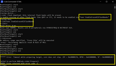
Dear Support Team,
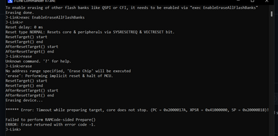
I am getting error while erasing the IMX1052 board and following is the error:
Below are the logs:
J-Link uptime (since boot): 0d 00h 22m 13s
S/N: 505103350
License(s): RDI, FlashBP, FlashDL, JFlash, GDB
USB speed mode: High speed (480 MBit/s)
VTref=3.286V
Type "connect" to establish a target connection, '?' for help
J-Link>connect
Please specify device / core. <Default>: MIMXRT1051XXXXA
Type '?' for selection dialog
Device>?
Please specify target interface:
J) JTAG (Default)
S) SWD
T) cJTAG
TIF>S
Specify target interface speed [kHz]. <Default>: 4000 kHz
Speed>
Device "MIMXRT1052XXXXB" selected.
Connecting to target via SWD
Found SW-DP with ID 0x0BD11477
DPIDR: 0x0BD11477
CoreSight SoC-400 or earlier
Scanning AP map to find all available APs
AP[1]: Stopped AP scan as end of AP map has been reached
AP[0]: AHB-AP (IDR: 0x04770041)
Iterating through AP map to find AHB-AP to use
AP[0]: Core found
AP[0]: AHB-AP ROM base: 0xE00FD000
CPUID register: 0x411FC271. Implementer code: 0x41 (ARM)
Found Cortex-M7 r1p1, Little endian.
FPUnit: 8 code (BP) slots and 0 literal slots
CoreSight components:
ROMTbl[0] @ E00FD000
[0][0]: E00FE000 CID B105100D PID 000BB4C8 ROM Table
ROMTbl[1] @ E00FE000
[1][0]: E00FF000 CID B105100D PID 000BB4C7 ROM Table
ROMTbl[2] @ E00FF000
[2][0]: E000E000 CID B105E00D PID 000BB00C SCS-M7
[2][1]: E0001000 CID B105E00D PID 000BB002 DWT
[2][2]: E0002000 CID B105E00D PID 000BB00E FPB-M7
[2][3]: E0000000 CID B105E00D PID 000BB001 ITM
[1][1]: E0041000 CID B105900D PID 001BB975 ETM-M7
[1][2]: E0042000 CID B105900D PID 004BB906 CTI
[0][1]: E0040000 CID B105900D PID 000BB9A9 TPIU-M7
[0][2]: E0043000 CID B105F00D PID 001BB101 TSG
Cache: Separate I- and D-cache.
I-Cache L1: 32 KB, 512 Sets, 32 Bytes/Line, 2-Way
D-Cache L1: 32 KB, 256 Sets, 32 Bytes/Line, 4-Way
Memory zones:
Zone: Default Description: Default access mode
Cortex-M7 identified.
J-Link>erase
No address range specified, 'Erase Chip' will be executed
'erase': Performing implicit reset & halt of MCU.
ResetTarget() start
ResetTarget() end
AfterResetTarget() start
AfterResetTarget() end
Erasing device...
J-Link: Flash download: Only internal flash banks will be erased.
To enable erasing of other flash banks like QSPI or CFI, it needs to be enabled via "exec EnableEraseAllFlashBanks"
Erasing done.
J-Link>exec EnableEraseAllFlashBanks
J-Link>r
Reset delay: 0 ms
Reset type NORMAL: Resets core & peripherals via SYSRESETREQ & VECTRESET bit.
ResetTarget() start
ResetTarget() end
AfterResetTarget() start
AfterResetTarget() end
J-Link>erase
No address range specified, 'Erase Chip' will be executed
'erase': Performing implicit reset & halt of MCU.
ResetTarget() start
ResetTarget() end
AfterResetTarget() start
AfterResetTarget() end
Erasing device...
****** Error: Timeout while preparing target, core does not stop. (PC = 0x2000017A, XPSR = 0x41000000, SP = 0x20000B18)!
Failed to perform RAMCode-sided Prepare()
ERROR: Erase returned with error code -1.
J-Link>
Let me know if you need more information.
Regards,
Sunil
