
- Forums
- Product Forums
- General Purpose MicrocontrollersGeneral Purpose Microcontrollers
- i.MX Forumsi.MX Forums
- QorIQ Processing PlatformsQorIQ Processing Platforms
- Identification and SecurityIdentification and Security
- Power ManagementPower Management
- Wireless ConnectivityWireless Connectivity
- RFID / NFCRFID / NFC
- Advanced AnalogAdvanced Analog
- Neural Processing UnitsNeural Processing Units
- MCX Microcontrollers
- S32G
- S32K
- S32V
- MPC5xxx
- Other NXP Products
- S12 / MagniV Microcontrollers
- Powertrain and Electrification Analog Drivers
- Sensors
- Vybrid Processors
- Digital Signal Controllers
- 8-bit Microcontrollers
- ColdFire/68K Microcontrollers and Processors
- PowerQUICC Processors
- OSBDM and TBDML
- S32M
- S32Z/E
-
- Solution Forums
- Software Forums
- MCUXpresso Software and ToolsMCUXpresso Software and Tools
- CodeWarriorCodeWarrior
- MQX Software SolutionsMQX Software Solutions
- Model-Based Design Toolbox (MBDT)Model-Based Design Toolbox (MBDT)
- FreeMASTER
- eIQ Machine Learning Software
- Embedded Software and Tools Clinic
- S32 SDK
- S32 Design Studio
- GUI Guider
- Zephyr Project
- Voice Technology
- Application Software Packs
- Secure Provisioning SDK (SPSDK)
- Processor Expert Software
- Generative AI & LLMs
-
- Topics
- Mobile Robotics - Drones and RoversMobile Robotics - Drones and Rovers
- NXP Training ContentNXP Training Content
- University ProgramsUniversity Programs
- Rapid IoT
- NXP Designs
- SafeAssure-Community
- OSS Security & Maintenance
- Using Our Community
-
- Cloud Lab Forums
-
- Knowledge Bases
- ARM Microcontrollers
- i.MX Processors
- Identification and Security
- Model-Based Design Toolbox (MBDT)
- QorIQ Processing Platforms
- S32 Automotive Processing Platform
- Wireless Connectivity
- CodeWarrior
- MCUXpresso Suite of Software and Tools
- MQX Software Solutions
- RFID / NFC
- Advanced Analog
- Neural Processing Units
-
- NXP Tech Blogs
- Home
- :
- i.MX Forums
- :
- i.MX Processors
- :
- Re: i.mx6ulz Default SD pins for eFuse Boot
i.mx6ulz Default SD pins for eFuse Boot
- Subscribe to RSS Feed
- Mark Topic as New
- Mark Topic as Read
- Float this Topic for Current User
- Bookmark
- Subscribe
- Mute
- Printer Friendly Page

- Mark as New
- Bookmark
- Subscribe
- Mute
- Subscribe to RSS Feed
- Permalink
- Report Inappropriate Content
Hi,
I posted this previously and it was confirmed from nxp that for eFuses to work, we must have the default SD2 pins assigned to the SD slot to boot from SD 2 with eFuses. : https://community.nxp.com/t5/i-MX-Processors/I-MX6ULZ-eFuse-boot-from-SD-with-custom-pinmux-for-SD-s...
However, now we are attempting to make the changes on our board and are having a difficult time understanding which actually the default SD2 slot pins are.
So as an example lets take SD2_CLK signal. Based on the RM the USDHC2 CLK can be routed to SD2_CLK, GPIO3_IO24, and NAND_RE_B pins/pads. But ALT1 mode is for only SD2_CLK and NAND_RE_B. We used SD2_CLK as this seems like the default SD2 clock pin. However, on the 6ull EVK they are actually using the NAND_RE_B for SD2_CLK and similarly the rest of the SD2 signals are also different and related to NAND instead of SD2 (e.g NAND_WE_B instead of SD2_CMD).
We blew the eFuses and the fuse values were read correct afterwards but could not boot to u-boot or OS. We can boot the OS fine via Serial downloader mode so all other operations are verified to work. Fuse values set and read below.
fuse prog 0 6 0x10
fuse prog 0 5 0x2840
So, ultimately our question is, which are the default pins for the SD2 signals that the ROM code looks in order to boot? the SD2_XXX or NAND_XXXX? If it is NAND_XXX, why is it that one? Or does it look at both?
The reference manual table :
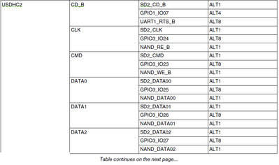
And our schematics for SD2 slot is as follows:
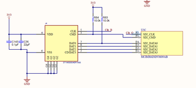
Reference design Schematic snippet from the EVK schematic file.

Solved! Go to Solution.

 igorpadykov
- Mark as New
- Bookmark
- Subscribe
- Mute
- Subscribe to RSS Feed
- Permalink
- Report Inappropriate Content
Hi Angshu
default SD pins for boot are described in sect.8.5.3.4 IOMUX configuration for SD/MMC
i.MX 6ULZ Applications Processor Reference Manual
Best regards
igor
igorpadykov
- Mark as New
- Bookmark
- Subscribe
- Mute
- Subscribe to RSS Feed
- Permalink
- Report Inappropriate Content
Hi Angshu
default SD pins for boot are described in sect.8.5.3.4 IOMUX configuration for SD/MMC
i.MX 6ULZ Applications Processor Reference Manual
Best regards
igor
- Mark as New
- Bookmark
- Subscribe
- Mute
- Subscribe to RSS Feed
- Permalink
- Report Inappropriate Content
Hi Igor,
Follow up question regarding this. Currently we have CLK, CMD, Data00 - 03 lines connected for SD.
We are rerouting it now as follows :
Signal Pin Pad
USDCH2_CLK NAND_RE_B D8
USDCH2_CMD NAND_WE_B C8
USDCH2_DATA0 NAND_DATA00 D7
USDCH2_DATA1 NAND_DATA01 B7
USDCH2_DATA2 NAND_DATA02 A7
USDCH2_DATA3 NAND_DATA03 D6
Will this be enough for the ROM to boot from our SD2 slot or do we need to connect other sd2 related signals that we do not use at the moment such as these below?
DATA4 NAND_DATA04
DATA5 NAND_DATA05
DATA6 NAND_DATA06
DATA7 NAND_DATA07
VSELECT GPIO1_IO08
RESET_B NAND_ALE
igorpadykov
- Mark as New
- Bookmark
- Subscribe
- Mute
- Subscribe to RSS Feed
- Permalink
- Report Inappropriate Content
yes this is enough for ROM to boot from SD2.
Best regards
igor
- Mark as New
- Bookmark
- Subscribe
- Mute
- Subscribe to RSS Feed
- Permalink
- Report Inappropriate Content
Hi Igor,
Thank you for the answer. We just ran into that table after posting here. Much appreciated.
