- Forums
- Product Forums
- General Purpose MicrocontrollersGeneral Purpose Microcontrollers
- i.MX Forumsi.MX Forums
- QorIQ Processing PlatformsQorIQ Processing Platforms
- Identification and SecurityIdentification and Security
- Power ManagementPower Management
- Wireless ConnectivityWireless Connectivity
- RFID / NFCRFID / NFC
- MCX Microcontrollers
- S32G
- S32K
- S32V
- MPC5xxx
- Other NXP Products
- S12 / MagniV Microcontrollers
- Powertrain and Electrification Analog Drivers
- Sensors
- Vybrid Processors
- Digital Signal Controllers
- 8-bit Microcontrollers
- ColdFire/68K Microcontrollers and Processors
- PowerQUICC Processors
- OSBDM and TBDML
- S32M
-
- Solution Forums
- Software Forums
- MCUXpresso Software and ToolsMCUXpresso Software and Tools
- CodeWarriorCodeWarrior
- MQX Software SolutionsMQX Software Solutions
- Model-Based Design Toolbox (MBDT)Model-Based Design Toolbox (MBDT)
- FreeMASTER
- eIQ Machine Learning Software
- Embedded Software and Tools Clinic
- S32 SDK
- S32 Design Studio
- GUI Guider
- Zephyr Project
- Voice Technology
- Application Software Packs
- Secure Provisioning SDK (SPSDK)
- Processor Expert Software
-
- Topics
- Mobile Robotics - Drones and RoversMobile Robotics - Drones and Rovers
- NXP Training ContentNXP Training Content
- University ProgramsUniversity Programs
- Rapid IoT
- NXP Designs
- SafeAssure-Community
- OSS Security & Maintenance
- Using Our Community
-
- Cloud Lab Forums
-
- Knowledge Bases
- ARM Microcontrollers
- i.MX Processors
- Identification and Security
- Model-Based Design Toolbox (MBDT)
- QorIQ Processing Platforms
- S32 Automotive Processing Platform
- Wireless Connectivity
- CodeWarrior
- MCUXpresso Suite of Software and Tools
- MQX Software Solutions
- RFID / NFC
-
I do not think, that this is good idea to violate PCB design recommendations, having a hope
to adjust timing requirements later via calibration. General considerations are as following.
There are two approaches regarding PCB design. Basically, the best approach - to use
simulation technique. In the same time, general rules (as the second approach) may be
provided for customers to simplify their PCB considerations, but note, for assurance such
rules are very strong.
So, if You can simulate the PCB design please use it, if cannot - please follow
general (and more strong) recommendations, such as provided in app note(s) or
in Hardware Development Guide.
Have a great day,
Yuri
-----------------------------------------------------------------------------------------------------------------------
Note: If this post answers your question, please click the Correct Answer button. Thank you!
-----------------------------------------------------------------------------------------------------------------------
Really the calibration helps for fine tuning, when base PCB design rules
are not violated. So, please try to follow design recommendations.
Have a great day,
Yuri
-----------------------------------------------------------------------------------------------------------------------
Note: If this post answers your question, please click the Correct Answer button. Thank you!
-----------------------------------------------------------------------------------------------------------------------
Yuri,
This is really where my question come from
-- per Hardware Guide of i.mx6, Table 3-3. DDR3 routing by byte group, it say "Match the signals of each byte group ± 25 mils". so we need to match the length of DQS with byte lines within ± 25 mils.
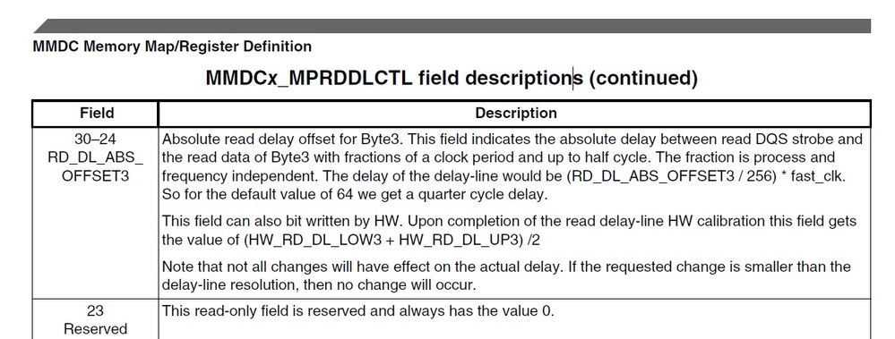
And per IMX6DQRM, MMDCx_MPRDDLCTL field descriptions, it say "This field indicates the absolute delay between read DQS strobe and the read data of Byte3 with fractions of a clock period and up to half cycle".
so the DDR controller can adjust the delay line for 127 steps in accuracy of 1/256 Tclk for each step. Typically the Tclk equal to 1ns for a 533MHz DDR3 system. That would make the adjust step in
4ps, and equal to 25 mils in a typical PCB flight time model.
Since we already route the DQS in ± 25 mils with byte lines, so why we still need to do read or write calibration, if our base PCB layout rules are not violated?
A wider margin than ± 25 mils, would benefit us a lot for DQS routing.
I do not think, that this is good idea to violate PCB design recommendations, having a hope
to adjust timing requirements later via calibration. General considerations are as following.
There are two approaches regarding PCB design. Basically, the best approach - to use
simulation technique. In the same time, general rules (as the second approach) may be
provided for customers to simplify their PCB considerations, but note, for assurance such
rules are very strong.
So, if You can simulate the PCB design please use it, if cannot - please follow
general (and more strong) recommendations, such as provided in app note(s) or
in Hardware Development Guide.
Have a great day,
Yuri
-----------------------------------------------------------------------------------------------------------------------
Note: If this post answers your question, please click the Correct Answer button. Thank you!
-----------------------------------------------------------------------------------------------------------------------
I do not think, that this is good idea to violate PCB design recommendations, having a hope
to adjust timing requirements later via calibration.
Could you tell us what purpose for read&write calibration feature designed for? According DQRM, there is up to 1/2 clock period for delay line tuning. If I can simulate my PCB design, or follow your recommendations, then this calibration is useless?

