- Forums
- Product Forums
- General Purpose MicrocontrollersGeneral Purpose Microcontrollers
- i.MX Forumsi.MX Forums
- QorIQ Processing PlatformsQorIQ Processing Platforms
- Identification and SecurityIdentification and Security
- Power ManagementPower Management
- Wireless ConnectivityWireless Connectivity
- RFID / NFCRFID / NFC
- Advanced AnalogAdvanced Analog
- MCX Microcontrollers
- S32G
- S32K
- S32V
- MPC5xxx
- Other NXP Products
- S12 / MagniV Microcontrollers
- Powertrain and Electrification Analog Drivers
- Sensors
- Vybrid Processors
- Digital Signal Controllers
- 8-bit Microcontrollers
- ColdFire/68K Microcontrollers and Processors
- PowerQUICC Processors
- OSBDM and TBDML
- S32M
- S32Z/E
-
- Solution Forums
- Software Forums
- MCUXpresso Software and ToolsMCUXpresso Software and Tools
- CodeWarriorCodeWarrior
- MQX Software SolutionsMQX Software Solutions
- Model-Based Design Toolbox (MBDT)Model-Based Design Toolbox (MBDT)
- FreeMASTER
- eIQ Machine Learning Software
- Embedded Software and Tools Clinic
- S32 SDK
- S32 Design Studio
- GUI Guider
- Zephyr Project
- Voice Technology
- Application Software Packs
- Secure Provisioning SDK (SPSDK)
- Processor Expert Software
- Generative AI & LLMs
-
- Topics
- Mobile Robotics - Drones and RoversMobile Robotics - Drones and Rovers
- NXP Training ContentNXP Training Content
- University ProgramsUniversity Programs
- Rapid IoT
- NXP Designs
- SafeAssure-Community
- OSS Security & Maintenance
- Using Our Community
-
- Cloud Lab Forums
-
- Knowledge Bases
- ARM Microcontrollers
- i.MX Processors
- Identification and Security
- Model-Based Design Toolbox (MBDT)
- QorIQ Processing Platforms
- S32 Automotive Processing Platform
- Wireless Connectivity
- CodeWarrior
- MCUXpresso Suite of Software and Tools
- MQX Software Solutions
- RFID / NFC
- Advanced Analog
-
- NXP Tech Blogs
- Home
- :
- i.MX Forums
- :
- i.MX Processors
- :
- i.MX8M memory setup/testing
i.MX8M memory setup/testing
- Subscribe to RSS Feed
- Mark Topic as New
- Mark Topic as Read
- Float this Topic for Current User
- Bookmark
- Subscribe
- Mute
- Printer Friendly Page
i.MX8M memory setup/testing
- Mark as New
- Bookmark
- Subscribe
- Mute
- Subscribe to RSS Feed
- Permalink
- Report Inappropriate Content
I have a query in relation the MX8M_LPDDR4_RPA_v24.xlsx
https://community.nxp.com/servlet/JiveServlet/download/340179-59-456897/MX8M_LPDDR4_RPA_v24.xlsx
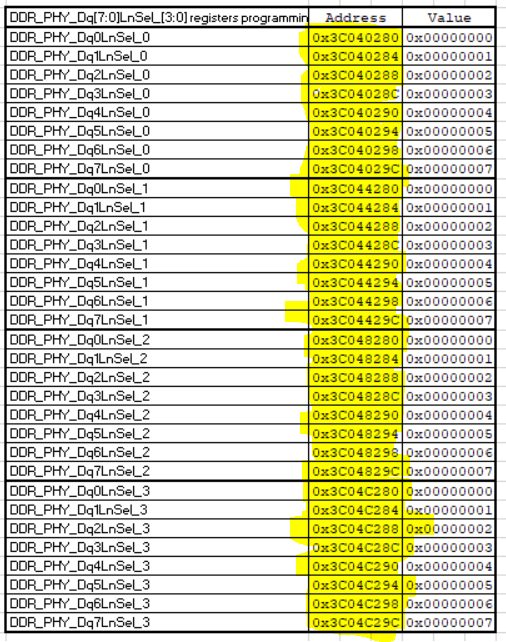
It lists the following DDR PHY addresses.
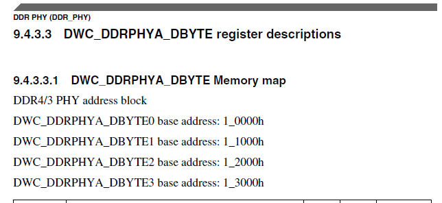
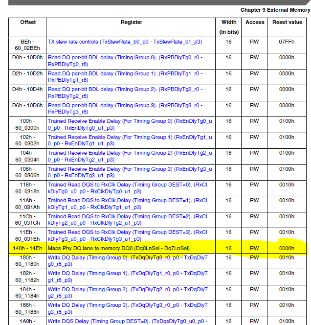
However the i.MX8M TRM (Rev. 2 08/2019) lists the PHY_DqnSel address as below (i.e DDR_PHY_DQ0LnSel_0 would be 0x3c010140?)
These definitions seem to be at odds with one another. Which one is correct? Or, am I missing something?
Regards,
PJ Nee.
- Mark as New
- Bookmark
- Subscribe
- Mute
- Subscribe to RSS Feed
- Permalink
- Report Inappropriate Content
Hello PJ Nee,
Please do use the addresses shown on the programming aid spreadsheet. The discrepancy seems to be related to the fact that the documentation for the DDR controller uses 16 bit addresses, as the memory map is part of Synopsys intellectual property.
My apologies for the inconvenience.
Regards,
- Mark as New
- Bookmark
- Subscribe
- Mute
- Subscribe to RSS Feed
- Permalink
- Report Inappropriate Content
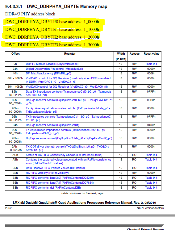
Ok - but I then have to question all the other PHY addresses in the i.MX8M TRM? Are they also wrong?
As an example take the DWC_DDRPHYA_DBYTE Memory map table below. Are the base addresses and offsets also all wrong?
- Mark as New
- Bookmark
- Subscribe
- Mute
- Subscribe to RSS Feed
- Permalink
- Report Inappropriate Content
Hello PJ Nee,
This seems to apply to all DDR PHY values. I inquired internally and the register offset values are already multiplied by 2 in the reference manual in comparison to the DDR PHY documentation. Therefore, if reference manual is used the final address is derived as follows:
address = DDR PHY base address + PHY block address*4 + register offset*2
So for example Dq0lnSel_0:
address = 0x3C00_0000 + 0x1_0000 * 4 + 0x140 * 2 = 0x3C04_0280
I hope this helps!
Regards,


