- Forums
- Product Forums
- General Purpose MicrocontrollersGeneral Purpose Microcontrollers
- i.MX Forumsi.MX Forums
- QorIQ Processing PlatformsQorIQ Processing Platforms
- Identification and SecurityIdentification and Security
- Power ManagementPower Management
- Wireless ConnectivityWireless Connectivity
- RFID / NFCRFID / NFC
- Advanced AnalogAdvanced Analog
- MCX Microcontrollers
- S32G
- S32K
- S32V
- MPC5xxx
- Other NXP Products
- S12 / MagniV Microcontrollers
- Powertrain and Electrification Analog Drivers
- Sensors
- Vybrid Processors
- Digital Signal Controllers
- 8-bit Microcontrollers
- ColdFire/68K Microcontrollers and Processors
- PowerQUICC Processors
- OSBDM and TBDML
- S32M
- S32Z/E
-
- Solution Forums
- Software Forums
- MCUXpresso Software and ToolsMCUXpresso Software and Tools
- CodeWarriorCodeWarrior
- MQX Software SolutionsMQX Software Solutions
- Model-Based Design Toolbox (MBDT)Model-Based Design Toolbox (MBDT)
- FreeMASTER
- eIQ Machine Learning Software
- Embedded Software and Tools Clinic
- S32 SDK
- S32 Design Studio
- GUI Guider
- Zephyr Project
- Voice Technology
- Application Software Packs
- Secure Provisioning SDK (SPSDK)
- Processor Expert Software
- Generative AI & LLMs
-
- Topics
- Mobile Robotics - Drones and RoversMobile Robotics - Drones and Rovers
- NXP Training ContentNXP Training Content
- University ProgramsUniversity Programs
- Rapid IoT
- NXP Designs
- SafeAssure-Community
- OSS Security & Maintenance
- Using Our Community
-
- Cloud Lab Forums
-
- Knowledge Bases
- ARM Microcontrollers
- i.MX Processors
- Identification and Security
- Model-Based Design Toolbox (MBDT)
- QorIQ Processing Platforms
- S32 Automotive Processing Platform
- Wireless Connectivity
- CodeWarrior
- MCUXpresso Suite of Software and Tools
- MQX Software Solutions
- RFID / NFC
- Advanced Analog
-
- NXP Tech Blogs
- Home
- :
- i.MX Forums
- :
- i.MX Processors
- :
- Slew rate failure while DDR3 read burst validation
Slew rate failure while DDR3 read burst validation
- Subscribe to RSS Feed
- Mark Topic as New
- Mark Topic as Read
- Float this Topic for Current User
- Bookmark
- Subscribe
- Mute
- Printer Friendly Page
Slew rate failure while DDR3 read burst validation
- Mark as New
- Bookmark
- Subscribe
- Mute
- Subscribe to RSS Feed
- Permalink
- Report Inappropriate Content
Hi All,
Currently I'm involving DDR3 validation.
Here is the information about my setup.
Processor : MCIMX6U6AVM08AC
DDR3 Memory : MT41K128M16JT-125AITK
DDR3 Clock frequency : 400MHz
ARM Frequency : 800MHz
Chip Select used : CS0
No of chip’s DDR3 chips used : 4 no’s connected in fly by topology
Oscilloscope : 16 GHZ DPO
Probing Points on the Processor:
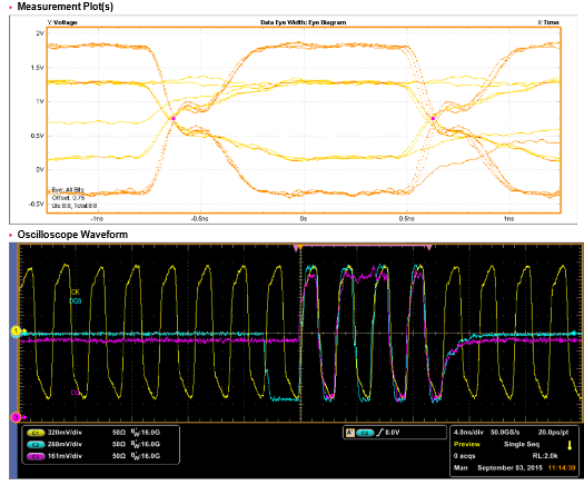
Clock (Channel C1) DDR_CLK_0 & DDR_CLK#_0
Data Strobe (Channel C2) DDR_SDQ0 & DDR_SDQ#0
Data 0 (Channel C3) DDR_DATA0
Observations:
We have done the below methods to make slew rate (SRQdiff & SRQse) pass in DDR Read Burst,
- Modified the ODT Termination with different values like 30 ,40 , 60 Ohms etc
- Modified the Drive strength of the DDR in MR1 register for DDR3
- Modified the Drive strength of Processor DQS , DQ which we are probing.
PS: We have calibrated the board with DDR3 stress test tool.
We are getting failure DQS slew rate measurements.
Can any one please help us to solve this problem.
- Mark as New
- Bookmark
- Subscribe
- Mute
- Subscribe to RSS Feed
- Permalink
- Report Inappropriate Content
Hello,
You may try simulation a) on die and b) on pin.
And quite acceptable waveforms on die look not so good on pin,
just as yours. It is important to have proper signals on die.
Have a great day,
Yuri
-----------------------------------------------------------------------------------------------------------------------
Note: If this post answers your question, please click the Correct Answer button. Thank you!
-----------------------------------------------------------------------------------------------------------------------
- Mark as New
- Bookmark
- Subscribe
- Mute
- Subscribe to RSS Feed
- Permalink
- Report Inappropriate Content
Hi,
according to the picture you do have a reflection on your measured signal. Most likly due to your testpoint. So this is a measurement artefact.
Are you using any interposer and do any de-embedding ?
But I have to admit, that I do not understand the Report from the Tek scope.
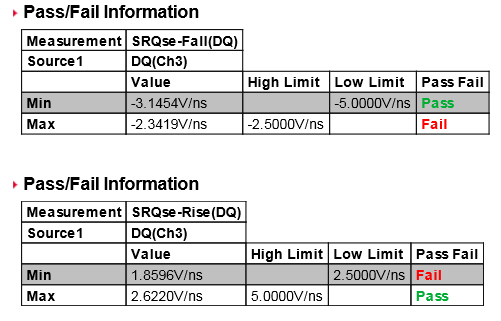
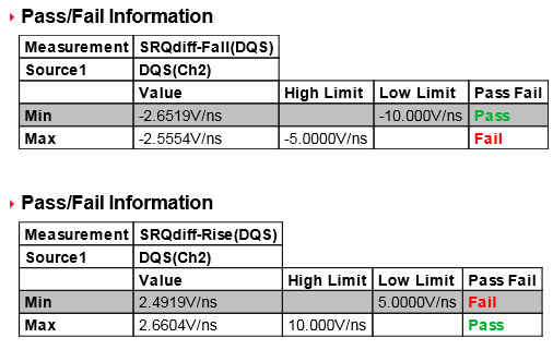
standard slew rate on DDR2 is still 1v/ns. not sure what the 5V/ns and 10V/ns really stand for and I'm also not sure why some of them are pass if you do not reach the low limit ..
But I have to admit, that I usually work with the tools from other scope vendors.
I would not expect that Tek does have better tools, so expect also wrong measurements ..
Hermann
- Mark as New
- Bookmark
- Subscribe
- Mute
- Subscribe to RSS Feed
- Permalink
- Report Inappropriate Content
Hi Hermann,
Thanks for your reply.
I don'see any wrong pass/fail here, I think that is -ve values right so more negative value means low and less negative value means high right?
So it seems measurement are correct.
PS: We able to make write burst pass.
Any recommendations ?
Thanks for your support.


