- Forums
- Product Forums
- General Purpose MicrocontrollersGeneral Purpose Microcontrollers
- i.MX Forumsi.MX Forums
- QorIQ Processing PlatformsQorIQ Processing Platforms
- Identification and SecurityIdentification and Security
- Power ManagementPower Management
- Wireless ConnectivityWireless Connectivity
- RFID / NFCRFID / NFC
- Advanced AnalogAdvanced Analog
- Neural Processing UnitsNeural Processing Units
- MCX Microcontrollers
- S32G
- S32K
- S32V
- MPC5xxx
- Other NXP Products
- S12 / MagniV Microcontrollers
- Powertrain and Electrification Analog Drivers
- Sensors
- Vybrid Processors
- Digital Signal Controllers
- 8-bit Microcontrollers
- ColdFire/68K Microcontrollers and Processors
- PowerQUICC Processors
- OSBDM and TBDML
- S32M
- S32Z/E
-
- Solution Forums
- Software Forums
- MCUXpresso Software and ToolsMCUXpresso Software and Tools
- CodeWarriorCodeWarrior
- MQX Software SolutionsMQX Software Solutions
- Model-Based Design Toolbox (MBDT)Model-Based Design Toolbox (MBDT)
- FreeMASTER
- eIQ Machine Learning Software
- Embedded Software and Tools Clinic
- S32 SDK
- S32 Design Studio
- GUI Guider
- Zephyr Project
- Voice Technology
- Application Software Packs
- Secure Provisioning SDK (SPSDK)
- Processor Expert Software
- Generative AI & LLMs
-
- Topics
- Mobile Robotics - Drones and RoversMobile Robotics - Drones and Rovers
- NXP Training ContentNXP Training Content
- University ProgramsUniversity Programs
- Rapid IoT
- NXP Designs
- SafeAssure-Community
- OSS Security & Maintenance
- Using Our Community
-
- Cloud Lab Forums
-
- Knowledge Bases
- ARM Microcontrollers
- i.MX Processors
- Identification and Security
- Model-Based Design Toolbox (MBDT)
- QorIQ Processing Platforms
- S32 Automotive Processing Platform
- Wireless Connectivity
- CodeWarrior
- MCUXpresso Suite of Software and Tools
- MQX Software Solutions
- RFID / NFC
- Advanced Analog
- Neural Processing Units
-
- NXP Tech Blogs
Sabresd Customed board, DDR stress test Fail

Custom board based on IMX6QP Sabresd , fly-by DDR3 Topolgy , DDR stress test Fail!
1,While running memtester app on Linux 3.14.52 kernel, I got following test failure (some time):
memtester version 4.3.0 (32-bit)
Copyright (C) 2001-2012 Charles Cazabon.
Licensed under the GNU General Public License version 2 (only).
pagesize is 4096
pagesizemask is 0xfffff000
want 1MB (1048576 bytes)
got 1MB (1048576 bytes), trying mlock ...locked.
Loop 1/1:
Stuck Address : ok
Random Value : ok
Compare XOR : ok
Compare SUB : ok
Compare MUL : ok
Compare DIV : ok
Compare OR : ok
Compare AND : ok
Sequential Increment: ok
Solid Bits : ok
Block Sequential : testing 60FAILURE: 0x3c3c3c3c != 0x3a3a3a3a at offset 0x0000021c.
FAILURE: 0x3c3c3c3c != 0x3a3a3a3a at offset 0x00000220.
FAILURE: 0x3c3c3c3c != 0x3a3a3a3a at offset 0x00000224.
FAILURE: 0x3c3c3c3c != 0x3a3a3a3a at offset 0x00000228.
FAILURE: 0x3c3c3c3c != 0x3a3a3a3a at offset 0x0000022c.
FAILURE: 0x3c3c3c3c != 0x3a3a3a3a at offset 0x00000230.
FAILURE: 0x3c3c3c3c != 0x3a3a3a3a at offset 0x00000234.
FAILURE: 0x3c3c3c3c != 0x3a3a3a3a at offset 0x00000238.
2,Then , I try to test the hardware Reference to i.MX6/7 DDR Stress Test Tool V3.00 , I can not get the DDR3 stress Test steady-pass! Even some time , the testing can pass one time, but when I press the test button again, it fail!
some time Pass:
DDR Freq: 396 MHz
t0.1: data is addr test
t0: memcpy10 SSN x64 test
t1: memcpy8 SSN x64 test
t2: byte-wise SSN x64 test
t3: memcpy11 random pattern test
t4: IRAM_to_DDRv2 test
t5: IRAM_to_DDRv1 test
t6: read noise walking ones and zeros test
3,But , I got very often as follows:
Loop 1:
DDR Freq: 396 MHz
t0.1: data is addr test
t0: memcpy10 SSN x64 test
Address of bank2 failure: 0x2c65d600
Data initially read was: 0x2C65D6042C65D600
Data re-read is: 0x2C65D6042C65D600
But pattern was: 0x0000000000000000
Error: failed to run stress test!!!
Loop2:
DDR Freq: 396 MHz
t0.1: data is addr test
t0: memcpy10 SSN x64 test
t1: memcpy8 SSN x64 test
t2: byte-wise SSN x64 test
t3: memcpy11 random pattern test
test2 Address: 0x2dadd5c0
Data initally read was: 0x55555555
Data re-read is: 0x55555555
But pattern was: 0xe2f2b504
Bit location: 0xb7a7e051
Error: failed to run stress test!!!
loop 3:
DDR Freq: 396 MHz
t0.1: data is addr test
t0: memcpy10 SSN x64 test
Address of bank2 failure: 0x2c65d600
Data initially read was: 0x2C65D6042C65D600
Data re-read is: 0x2C65D6042C65D600
But pattern was: 0x0000000000000000
Error: failed to run stress test!!!
4,by the way, this is my first time using stress test tool, I tried GUI based option on NXP Sabresd (REVC) ,loading script file MX6Q_SabreSD_DDR3_1GB_64bit.inc ,It can not pass either! some software operation problem ?
5,my custom board(using Fly-by Topology,DDR3, 4 x MT41K128M16JT-125 :K), can you help me to fix the pameters or suggestions?
what does the following info mean and any suggestions?
t0.1: data is addr test
t0: memcpy10 SSN x64 test
Address of bank1 failure: 0x18941780
Data initially read was: 0x1894178418941780
Data re-read is: 0x1894178418941780
But pattern was: 0xFFFFFFFFFFFFFFFF
Error: failed to run stress test!!!@@@@

 igorpadykov
this means that ddr test sent data pattern : 0xFFFFFFFFFFFFFFFF
and expect read the same data, but instead read 0x1894178418941780.
This may point that ddr memory is not working at all, suggest to check
Freescale i.MX6 DRAM Port Application Guide-DDR3
Best regards
igor
U-boot mode, When the board start up, without loading the DDR Stress Test (3.0.0), I try to read and write the ADDR 0x18941780 ,It seems the ddr working as following.
Does the calibration tool suit for both T-Type and Fly-By type DDR PCB layout? If the board is Fly-by type, I have to set somewhere paramter to tell the cal tool?
Have I to set the drive strengh of the DDR ADDR and CMD PAD?
------------------------------------------------------------------
U-Boot 2017.03 (Aug 16 2019 - 12:09:33 +0800)
CPU: Freescale i.MX6QP rev1.0 996 MHz (running at 792 MHz)
CPU: Extended Commercial temperature grade (-20C to 105C) at 19C
Reset cause: POR
Board: MX6-SabreSD
I2C: ready
DRAM: 1 GiB
EIM Init here!
MMC: _zhtao:board_mmc_init=3:0
_zhtao:board_mmc_init=3:1
_zhtao:board_mmc_init=3:2
FSL_SDHC: 0, FSL_SDHC: 1, FSL_SDHC: 2
PCI: pcie phy link never came up
No panel detected: default to Hannstar-XGA
Display: Hannstar-XGA (1024x768)
In: serial
Out: serial
Err: serial
Net: FEC [PRIME]
Hit any key to stop autoboot: 0
=> mm 0x18941780
18941780: cfedfdf5 ? 55555555
18941784: f77d7bed ? -
18941780: 55555555 ? ffffffff
18941784: f77d7bed ? -
18941780: ffffffff ? .
=> md 0x18941780
18941780: ffffffff f77d7bed ecbe7efe fd3f98dd .....{}..~....?.
18941790: e3e37afd 407e70de 1ffafdbb ce7ebbf8 .z...p~@......~.
189417a0: acbcfcaf f91fa39f dfab71e7 7e9b394b .........q..K9.~
189417b0: eda3f165 79fae3df b64e7bdd 78cee7f2 e......y.{N....x
189417c0: 598251bc f63ac394 cceefd72 42e9d5ee .Q.Y..:.r......B
189417d0: 6f2fcada fcecb7c4 593dd26a 56b7d364 ../o....j.=Yd..V
189417e0: da9bee0f bbff6faf 6ff86cef ffcfb7a7 .....o...l.o....
189417f0: f6bb5afe f9ba7174 31bafb5f f5e6eecc .Z..tq.._..1....
18941800: 288eec0a fdbfd318 efefb3ea d0b522de ...(........."..
18941810: fabcd9c8 f7bbe2f7 fd6bb5cf 50f1ed8e ..........k....P
18941820: f1cf5cc3 687fd9eb eedaebb3 dfe4b3bf .\.....h........
18941830: f7b5b493 d5b6ba9f aece7dae bbef76d5 .........}...v..
18941840: 7f7ffd7f 25cbf4cb 7e6f07df 6bbef5fc .......%..o~...k
18941850: fe677dfe 6cb5d3ff dd39ce1a f3fbf65d .}g....l..9.]...
18941860: 7d3b71c7 f89f5af8 fa7fc7cd 3c3787aa .q;}.Z........7<
18941870: af3d4449 f9af7cff f33ea6fa dfbd26fb ID=..|....>..&..
igorpadykov
>Does the calibration tool suit for both T-Type and Fly-By type DDR PCB layout?
sorry Fly-By type is not supported by NXP, for its support recommended to proceed with
NXP Professional Services | NXP
Best regards
igor
I have got my custom board Pass @ GUI mode, But Fail @uboot mode using ddr_stress_tester_uboot_v3.00.
Is it because the hardware or ddr configuration problem?
What I have tried is turn the ddr frequency from default 528M to 396M by add
DATA 4 0x020c4018 0x00060324
at the beginning the mx6q_4x_mt41j128.cfg and generate the u-boot.imx file.
then I dow linke this:
=> dcache off
=> icache off
=> tftp 0x00907000 192.168.1.119:mx6dq.bin
Using FEC device
TFTP from server 192.168.1.119; our IP address is 192.168.1.76
Filename 'mx6dq.bin'.
Load address: 0x907000
Loading: ###T ######
1.3 MiB/s
done
Bytes transferred = 121880 (1dc18 hex)
=> go 0x907000
## Starting application at 0x00907000 ...
============================================
DDR Stress Test (3.0.0)
Build: Dec 14 2018, 14:20:05
NXP Semiconductors.
============================================
============================================
Chip ID
CHIP ID = i.MX6 Dual/Quad (0x63)
Internal Revision = TO2.0
============================================
============================================
Boot Configuration
SRC_SBMR1(0x020d8004) = 0x02005860
SRC_SBMR2(0x020d801c) = 0x2a000001
============================================
What ARM core speed would you like to run?
Type 1 for 800MHz, 2 for 1GHz, 3 for 1.2GHz
ARM Clock set to 800MHz
============================================
DDR configuration
BOOT_CFG3[5-4]: 0x00, Single DDR channel.
DDR type is DDR3
Data width: 64, bank num: 8
Row size: 14, col size: 10
Chip select CSD0 is used
Density per chip select: 1024MB
============================================
Current Temperature: 40
============================================
Please select the DDR density per chip select (in bytes) on the board
Type 0 for 2GB; 1 for 1GB; 2 for 512MB; 3 for 256MB; 4 for 128MB; 5 for 64MB; 6 for 32MB
For maximum supported density (4GB), we can only access up to 3.75GB. Type 7 to select this
DDR density selected (MB): 1024
Would do you want to change VDD_SOC_CAP/VDD_ARM_CAP voltage? Type 'y' to run and 'n' to skip
Would do you want run DDR Calibration? Type 'y' to run and 'n' to skip
Calibration will run at DDR frequency 528MHz. Type 'y' to continue.
If you want to run at other DDR frequency. Type 'n'
Enter the DDR frequency for calibration [350MHz to 528MHz]:
400
The freq you entered was: 400
Please enter the MR1 value on the initilization script
This will be re-programmed into MR1 after write leveling calibration
Enter as a 4-digit HEX value, example 0004, then hit enter
0004DDR Freq: 396 MHz
ddr_mr1=0x00000004
Start write leveling calibration...
running Write level HW calibration
MPWLHWERR register read out for factory diagnostics:
MPWLHWERR PHY0 = 0x3c3c1e1e
MPWLHWERR PHY1 = 0x3c3c3c3c
Write leveling calibration completed, update the following registers in your initialization script
MMDC_MPWLDECTRL0 ch0 (0x021b080c) = 0x001E001C
MMDC_MPWLDECTRL1 ch0 (0x021b0810) = 0x003A002C
MMDC_MPWLDECTRL0 ch1 (0x021b480c) = 0x00220035
MMDC_MPWLDECTRL1 ch1 (0x021b4810) = 0x0022002E
Write DQS delay result:
Write DQS0 delay: 28/256 CK
Write DQS1 delay: 30/256 CK
Write DQS2 delay: 44/256 CK
Write DQS3 delay: 58/256 CK
Write DQS4 delay: 53/256 CK
Write DQS5 delay: 34/256 CK
Write DQS6 delay: 46/256 CK
Write DQS7 delay: 34/256 CK
WARNING: write-leveling calibration value is greater than 1/8 CK.
Per the reference manual, WALAT must be set to 1 in the register MDMISC(0x021B0018).
This has been performed automatically.
However, in addition to updating the calibration values in your DDR initialization,
it is also REQUIRED change the value of MDMISC in their DDR initialization as follows:
MMDC_MDMISC (0x021b0018) = 0x00091740
Starting DQS gating calibration
. HC_DEL=0x00000000 result[00]=0x11111111
. HC_DEL=0x00000001 result[01]=0x11111111
. HC_DEL=0x00000002 result[02]=0x00000000
. HC_DEL=0x00000003 result[03]=0x00000000
. HC_DEL=0x00000004 result[04]=0x11111111
. HC_DEL=0x00000005 result[05]=0x11111111
. HC_DEL=0x00000006 result[06]=0x11111111
. HC_DEL=0x00000007 result[07]=0x11111111
. HC_DEL=0x00000008 result[08]=0x11111111
. HC_DEL=0x00000009 result[09]=0x11111111
. HC_DEL=0x0000000A result[0A]=0x11111111
. HC_DEL=0x0000000B result[0B]=0x11111111
. HC_DEL=0x0000000C result[0C]=0x11111111
. HC_DEL=0x0000000D result[0D]=0x11111111
DQS HC delay value low1 = 0x02020202, high1=0x03030303
DQS HC delay value low2 = 0x02020202, high2=0x03030303
loop ABS offset to get HW_DG_LOW
. ABS_OFFSET=0x00000000 result[00]=0x00111110
. ABS_OFFSET=0x00000004 result[01]=0x00111110
. ABS_OFFSET=0x00000008 result[02]=0x00111110
. ABS_OFFSET=0x0000000C result[03]=0x00111110
. ABS_OFFSET=0x00000010 result[04]=0x00111110
. ABS_OFFSET=0x00000014 result[05]=0x00111110
. ABS_OFFSET=0x00000018 result[06]=0x11111111
. ABS_OFFSET=0x0000001C result[07]=0x11111111
. ABS_OFFSET=0x00000020 result[08]=0x00111110
. ABS_OFFSET=0x00000024 result[09]=0x11111111
. ABS_OFFSET=0x00000028 result[0A]=0x00110110
. ABS_OFFSET=0x0000002C result[0B]=0x00110110
. ABS_OFFSET=0x00000030 result[0C]=0x11111111
. ABS_OFFSET=0x00000034 result[0D]=0x00110000
. ABS_OFFSET=0x00000038 result[0E]=0x11111111
. ABS_OFFSET=0x0000003C result[0F]=0x11111111
. ABS_OFFSET=0x00000040 result[10]=0x00000000
. ABS_OFFSET=0x00000044 result[11]=0x00000000
. ABS_OFFSET=0x00000048 result[12]=0x11111111
. ABS_OFFSET=0x0000004C result[13]=0x11111111
. ABS_OFFSET=0x00000050 result[14]=0x11111111
. ABS_OFFSET=0x00000054 result[15]=0x00000000
. ABS_OFFSET=0x00000058 result[16]=0x00000000
. ABS_OFFSET=0x0000005C result[17]=0x00000000
. ABS_OFFSET=0x00000060 result[18]=0x11111111
. ABS_OFFSET=0x00000064 result[19]=0x11111111
. ABS_OFFSET=0x00000068 result[1A]=0x00000000
. ABS_OFFSET=0x0000006C result[1B]=0x11111111
. ABS_OFFSET=0x00000070 result[1C]=0x11111111
. ABS_OFFSET=0x00000074 result[1D]=0x11111111
. ABS_OFFSET=0x00000078 result[1E]=0x00000000
. ABS_OFFSET=0x0000007C result[1F]=0x00000000
loop ABS offset to get HW_DG_HIGH
. ABS_OFFSET=0x00000000 result[00]=0x11111111
. ABS_OFFSET=0x00000004 result[01]=0x00000000
. ABS_OFFSET=0x00000008 result[02]=0x00000000
. ABS_OFFSET=0x0000000C result[03]=0x00000000
. ABS_OFFSET=0x00000010 result[04]=0x00000000
. ABS_OFFSET=0x00000014 result[05]=0x00000000
. ABS_OFFSET=0x00000018 result[06]=0x00000000
. ABS_OFFSET=0x0000001C result[07]=0x00000000
. ABS_OFFSET=0x00000020 result[08]=0x00000000
. ABS_OFFSET=0x00000024 result[09]=0x11111111
. ABS_OFFSET=0x00000028 result[0A]=0x00000000
. ABS_OFFSET=0x0000002C result[0B]=0x11111111
. ABS_OFFSET=0x00000030 result[0C]=0x11111111
. ABS_OFFSET=0x00000034 result[0D]=0x00000000
. ABS_OFFSET=0x00000038 result[0E]=0x00000000
. ABS_OFFSET=0x0000003C result[0F]=0x11111111
. ABS_OFFSET=0x00000040 result[10]=0x00000000
. ABS_OFFSET=0x00000044 result[11]=0x01000000
. ABS_OFFSET=0x00000048 result[12]=0x01000000
. ABS_OFFSET=0x0000004C result[13]=0x01000000
. ABS_OFFSET=0x00000050 result[14]=0x01001000
. ABS_OFFSET=0x00000054 result[15]=0x01001010
. ABS_OFFSET=0x00000058 result[16]=0x11111111
. ABS_OFFSET=0x0000005C result[17]=0x11111111
. ABS_OFFSET=0x00000060 result[18]=0x11101111
. ABS_OFFSET=0x00000064 result[19]=0x11111111
. ABS_OFFSET=0x00000068 result[1A]=0x11111111
. ABS_OFFSET=0x0000006C result[1B]=0x11111111
. ABS_OFFSET=0x00000070 result[1C]=0x11111111
. ABS_OFFSET=0x00000074 result[1D]=0x11111111
. ABS_OFFSET=0x00000078 result[1E]=0x11111111
. ABS_OFFSET=0x0000007C result[1F]=0x11111111
BYTE 0:
Start: HC=0x01 ABS=0x00
End: HC=0x03 ABS=0x20
Mean: HC=0x02 ABS=0x10
End-0.5*tCK: HC=0x02 ABS=0x20
Final: HC=0x02 ABS=0x20
BYTE 1:
Start: HC=0x01 ABS=0x54
End: HC=0x03 ABS=0x20
Mean: HC=0x02 ABS=0x3A
End-0.5*tCK: HC=0x02 ABS=0x20
Final: HC=0x02 ABS=0x3A
BYTE 2:
Start: HC=0x01 ABS=0x54
End: HC=0x03 ABS=0x20
Mean: HC=0x02 ABS=0x3A
End-0.5*tCK: HC=0x02 ABS=0x20
Final: HC=0x02 ABS=0x3A
BYTE 3:
Start: HC=0x01 ABS=0x54
End: HC=0x03 ABS=0x20
Mean: HC=0x02 ABS=0x3A
End-0.5*tCK: HC=0x02 ABS=0x20
Final: HC=0x02 ABS=0x3A
BYTE 4:
Start: HC=0x01 ABS=0x54
End: HC=0x03 ABS=0x20
Mean: HC=0x02 ABS=0x3A
End-0.5*tCK: HC=0x02 ABS=0x20
Final: HC=0x02 ABS=0x3A
BYTE 5:
Start: HC=0x01 ABS=0x54
End: HC=0x03 ABS=0x20
Mean: HC=0x02 ABS=0x3A
End-0.5*tCK: HC=0x02 ABS=0x20
Final: HC=0x02 ABS=0x3A
BYTE 6:
Start: HC=0x01 ABS=0x00
End: HC=0x03 ABS=0x20
Mean: HC=0x02 ABS=0x10
End-0.5*tCK: HC=0x02 ABS=0x20
Final: HC=0x02 ABS=0x20
BYTE 7:
Start: HC=0x01 ABS=0x00
End: HC=0x03 ABS=0x20
Mean: HC=0x02 ABS=0x10
End-0.5*tCK: HC=0x02 ABS=0x20
Final: HC=0x02 ABS=0x20
DQS calibration MMDC0 MPDGCTRL0 = 0x423A0220, MPDGCTRL1 = 0x023A023A
DQS calibration MMDC1 MPDGCTRL0 = 0x423A023A, MPDGCTRL1 = 0x02200220
Note: Array result[] holds the DRAM test result of each byte.
0: test pass. 1: test fail
4 bits respresent the result of 1 byte.
result 00000001:byte 0 fail.
result 00000011:byte 0, 1 fail.
Starting Read calibration...
ABS_OFFSET=0x00000000 result[00]=0x11111111
ABS_OFFSET=0x04040404 result[01]=0x11111111
ABS_OFFSET=0x08080808 result[02]=0x11111111
ABS_OFFSET=0x0C0C0C0C result[03]=0x11111111
ABS_OFFSET=0x10101010 result[04]=0x10011001
ABS_OFFSET=0x14141414 result[05]=0x00001000
ABS_OFFSET=0x18181818 result[06]=0x00001000
ABS_OFFSET=0x1C1C1C1C result[07]=0x00000000
ABS_OFFSET=0x20202020 result[08]=0x11111111
ABS_OFFSET=0x24242424 result[09]=0x00000000
ABS_OFFSET=0x28282828 result[0A]=0x00000000
ABS_OFFSET=0x2C2C2C2C result[0B]=0x00000000
ABS_OFFSET=0x30303030 result[0C]=0x00000000
ABS_OFFSET=0x34343434 result[0D]=0x00000000
ABS_OFFSET=0x38383838 result[0E]=0x11111111
ABS_OFFSET=0x3C3C3C3C result[0F]=0x00000000
ABS_OFFSET=0x40404040 result[10]=0x00000000
ABS_OFFSET=0x44444444 result[11]=0x00000000
ABS_OFFSET=0x48484848 result[12]=0x11111111
ABS_OFFSET=0x4C4C4C4C result[13]=0x00000000
ABS_OFFSET=0x50505050 result[14]=0x11111111
ABS_OFFSET=0x54545454 result[15]=0x00000000
ABS_OFFSET=0x58585858 result[16]=0x11111111
ABS_OFFSET=0x5C5C5C5C result[17]=0x00000000
ABS_OFFSET=0x60606060 result[18]=0x00000000
ABS_OFFSET=0x64646464 result[19]=0x00000000
ABS_OFFSET=0x68686868 result[1A]=0x00000000
ABS_OFFSET=0x6C6C6C6C result[1B]=0x01100000
ABS_OFFSET=0x70707070 result[1C]=0x01100100
ABS_OFFSET=0x74747474 result[1D]=0x01100111
ABS_OFFSET=0x78787878 result[1E]=0x11110111
ABS_OFFSET=0x7C7C7C7C result[1F]=0x11111111
Byte 0: (0x5c - 0x70), middle value:0x66
Byte 1: (0x5c - 0x70), middle value:0x66
Byte 2: (0x24 - 0x34), middle value:0x2c
Byte 3: (0x5c - 0x78), middle value:0x6a
Byte 4: (0x5c - 0x74), middle value:0x68
Byte 5: (0x24 - 0x34), middle value:0x2c
Byte 6: (0x24 - 0x34), middle value:0x2c
Byte 7: (0x5c - 0x74), middle value:0x68
MMDC0 MPRDDLCTL = 0x6A2C6666, MMDC1 MPRDDLCTL = 0x682C2C68
Starting Write calibration...
ABS_OFFSET=0x00000000 result[00]=0x11111111
ABS_OFFSET=0x04040404 result[01]=0x11111111
ABS_OFFSET=0x08080808 result[02]=0x10110111
ABS_OFFSET=0x0C0C0C0C result[03]=0x10100010
ABS_OFFSET=0x10101010 result[04]=0x11111111
ABS_OFFSET=0x14141414 result[05]=0x00000000
ABS_OFFSET=0x18181818 result[06]=0x00000000
ABS_OFFSET=0x1C1C1C1C result[07]=0x11111111
ABS_OFFSET=0x20202020 result[08]=0x00000000
ABS_OFFSET=0x24242424 result[09]=0x11111111
ABS_OFFSET=0x28282828 result[0A]=0x00000000
ABS_OFFSET=0x2C2C2C2C result[0B]=0x00000000
ABS_OFFSET=0x30303030 result[0C]=0x00000000
ABS_OFFSET=0x34343434 result[0D]=0x00000000
ABS_OFFSET=0x38383838 result[0E]=0x00000000
ABS_OFFSET=0x3C3C3C3C result[0F]=0x11111111
ABS_OFFSET=0x40404040 result[10]=0x00000000
ABS_OFFSET=0x44444444 result[11]=0x00000000
ABS_OFFSET=0x48484848 result[12]=0x00000000
ABS_OFFSET=0x4C4C4C4C result[13]=0x11111111
ABS_OFFSET=0x50505050 result[14]=0x00000000
ABS_OFFSET=0x54545454 result[15]=0x00000000
ABS_OFFSET=0x58585858 result[16]=0x00000000
ABS_OFFSET=0x5C5C5C5C result[17]=0x00000000
ABS_OFFSET=0x60606060 result[18]=0x00000000
ABS_OFFSET=0x64646464 result[19]=0x00000000
ABS_OFFSET=0x68686868 result[1A]=0x00000000
ABS_OFFSET=0x6C6C6C6C result[1B]=0x01000000
ABS_OFFSET=0x70707070 result[1C]=0x11111111
ABS_OFFSET=0x74747474 result[1D]=0x01001110
ABS_OFFSET=0x78787878 result[1E]=0x11111111
ABS_OFFSET=0x7C7C7C7C result[1F]=0x11111111
Byte 0: (0x50 - 0x6c), middle value:0x5e
Byte 1: (0x50 - 0x6c), middle value:0x5e
Byte 2: (0x50 - 0x6c), middle value:0x5e
Byte 3: (0x50 - 0x6c), middle value:0x5e
Byte 4: (0x50 - 0x6c), middle value:0x5e
Byte 5: (0x50 - 0x6c), middle value:0x5e
Byte 6: (0x50 - 0x68), middle value:0x5c
Byte 7: (0x50 - 0x6c), middle value:0x5e
MMDC0 MPWRDLCTL = 0x5E5E5E5E,MMDC1 MPWRDLCTL = 0x5E5C5E5E
MMDC registers updated from calibration
Write leveling calibration
MMDC_MPWLDECTRL0 ch0 (0x021b080c) = 0x001E001C
MMDC_MPWLDECTRL1 ch0 (0x021b0810) = 0x003A002C
MMDC_MPWLDECTRL0 ch1 (0x021b480c) = 0x00220035
MMDC_MPWLDECTRL1 ch1 (0x021b4810) = 0x0022002E
Read DQS Gating calibration
MPDGCTRL0 PHY0 (0x021b083c) = 0x423A0220
MPDGCTRL1 PHY0 (0x021b0840) = 0x023A023A
MPDGCTRL0 PHY1 (0x021b483c) = 0x423A023A
MPDGCTRL1 PHY1 (0x021b4840) = 0x02200220
Read calibration
MPRDDLCTL PHY0 (0x021b0848) = 0x6A2C6666
MPRDDLCTL PHY1 (0x021b4848) = 0x682C2C68
Write calibration
MPWRDLCTL PHY0 (0x021b0850) = 0x5E5E5E5E
MPWRDLCTL PHY1 (0x021b4850) = 0x5E5C5E5E
Success: DDR calibration completed!!!
The DDR stress test can run with an incrementing frequency or at a static freq
To run at a static freq, simply set the start freq and end freq to the same value
Would do you want run DDR Stress Test? Type 'y' to run and 'n' to skip
Enter desired START freq (135 to 672 MHz), then hit enter.
Note: DDR3 minimum is ~333MHz, do not recommend to go too much below this.
400
The freq you entered was: 400
Enter desired END freq (135 to 672 MHz), then hit enter.
Make sure this is equal to or greater than start freq
400
The freq you entered was: 400
Do you want to run DDR Stress Test for simple loop or Over Night Test?
Type '0' for simple loop. Type '1' for Over Night Test
DDR Stress Test Iteration 1
Current Temperature: 40
============================================
@DDR Freq: 396 MHz
t0.1: data is addr test
t0: memcpy10 SSN x64 test
Address of bank1 failure: 0x18941780
Data initially read was: 0x1894178418941780
Data re-read is: 0x1894178418941780
But pattern was: 0xFFFFFFFFFFFFFFFF
Error: failed to run stress test!!!@@@@
igorpadykov
Hi Zhao
one can try latest ddr test, MX6 Script Aids
i.MX6/7 DDR Stress Test Tool V3.00
Freescale i.MX6 DRAM Port Application Guide-DDR3
check board power supplies using
Best regards
igor
-----------------------------------------------------------------------------------------------------------------------
Note: If this post answers your question, please click the Correct Answer button. Thank you!
-----------------------------------------------------------------------------------------------------------------------
Thanks Igor,
This help me.
I have another question, now I have the memery test Pass using DDR_Tester.exe Then I get the *.inc file.
Then I modify the mx6q_4x_mt41j128.cfg.
When Some parameters change cause the board not booting up.
Does following parameters enough? As our custom baord is Fly-by topology.
// For target board, may need to run write leveling calibration to fine tune these settings.
setmem /32 0x021b080c = 0x0019000D
setmem /32 0x021b0810 = 0x003C002C
setmem /32 0x021b480c = 0x0023003C
setmem /32 0x021b4810 = 0x0021002C
////Read DQS Gating calibration
setmem /32 0x021b083c = 0x43340344 // MPDGCTRL0 PHY0
setmem /32 0x021b0840 = 0x03380338 // MPDGCTRL1 PHY0
setmem /32 0x021b483c = 0x43480350 // MPDGCTRL0 PHY1
setmem /32 0x021b4840 = 0x034C0324 // MPDGCTRL1 PHY1
//Read calibration
setmem /32 0x021b0848 = 0x4434363A // MPRDDLCTL PHY0
setmem /32 0x021b4848 = 0x3C36323C // MPRDDLCTL PHY1
//Write calibration
setmem /32 0x021b0850 = 0x3C3E424C // MPWRDLCTL PHY0
setmem /32 0x021b4850 = 0x4A404C44 // MPWRDLCTL PHY1
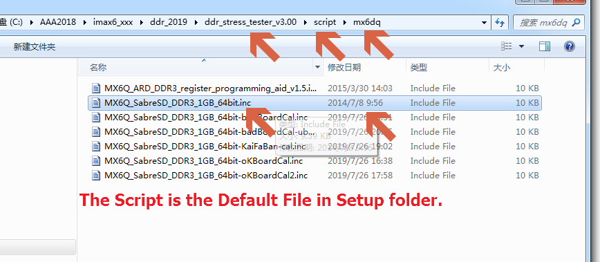
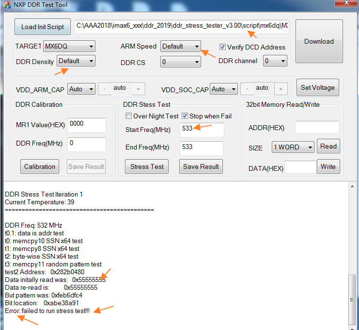
My cfg and inc file is as follow ,please help me check.
C:\AAA2018\imax6_xxx\ddr_2019\ddr_stress_tester_v3.00\mx6q_4x_mt41j128.cfg
C:\AAA2018\imax6_xxx\ddr_2019\ddr_stress_tester_v3.00\script\mx6dq\125ddr-528m-cp1a.inc
 igorpadykov
one can check presentation describing ddr test usage
DES-N1936 i.MX 6UltraLite DDR Tools Overview and Hardware Design Considerations
Best regards
igor
t0.1: data is addr test
t0: memcpy10 SSN x64 test
Address of bank1 failure: 0x18941780
Data initially read was: 0x1894178418941780
Data re-read is: 0x1894178418941780
But pattern was: 0xFFFFFFFFFFFFFFFF
Error: failed to run stress test!!
I wonder why it pass in GUI test but fail in Uboot mode
any suggestions?
Thanks igor,
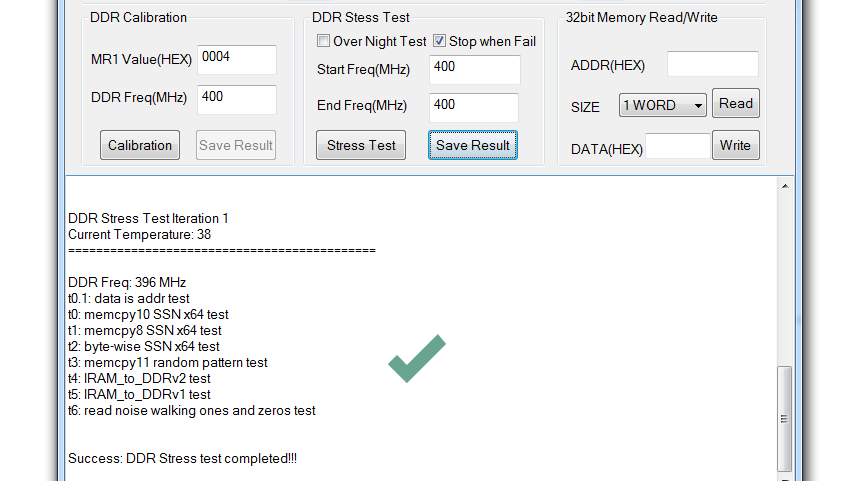
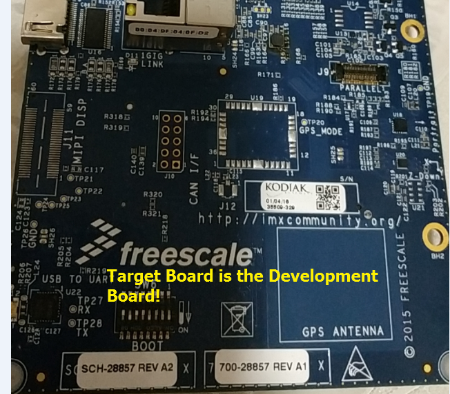
Now I can get the Developement board ddr press test Pass @400Mhz now, I have a question about the ddr frequency.
what the real frequency the ddr running at? How can I fix the value from the register or u-boot log?
If I get the test pass at 400Mhz Does it mean that the board can Run steday at 792Mhz of arm?
My boot log is as follows,
U-Boot 2017.03 (Apr 11 2019 - 16:03:32 +0800)
CPU: Freescale i.MX6QP rev1.0 996 MHz (running at 792 MHz)
CPU: Extended Commercial temperature grade (-20C to 105C) at 26C
Reset cause: POR
Board: MX6-SabreSD
I2C: ready
DRAM: 1 GiB
EIM Init here!
MMC: _zhtao:board_mmc_init=3:0
_zhtao:board_mmc_init=3:1
_zhtao:board_mmc_init=3:2
FSL_SDHC: 0, FSL_SDHC: 1, FSL_SDHC: 2
PCI: pcie phy link never came up
No panel detected: default to Hannstar-XGA
Display: Hannstar-XGA (1024x768)
In: serial
Out: serial
Err: serial
Net: FEC [PRIME]
Hit any key to stop autoboot: 0