
- Forums
- Product Forums
- General Purpose MicrocontrollersGeneral Purpose Microcontrollers
- i.MX Forumsi.MX Forums
- QorIQ Processing PlatformsQorIQ Processing Platforms
- Identification and SecurityIdentification and Security
- Power ManagementPower Management
- Wireless ConnectivityWireless Connectivity
- RFID / NFCRFID / NFC
- Advanced AnalogAdvanced Analog
- Neural Processing UnitsNeural Processing Units
- MCX Microcontrollers
- S32G
- S32K
- S32V
- MPC5xxx
- Other NXP Products
- S12 / MagniV Microcontrollers
- Powertrain and Electrification Analog Drivers
- Sensors
- Vybrid Processors
- Digital Signal Controllers
- 8-bit Microcontrollers
- ColdFire/68K Microcontrollers and Processors
- PowerQUICC Processors
- OSBDM and TBDML
- S32M
- S32Z/E
-
- Solution Forums
- Software Forums
- MCUXpresso Software and ToolsMCUXpresso Software and Tools
- CodeWarriorCodeWarrior
- MQX Software SolutionsMQX Software Solutions
- Model-Based Design Toolbox (MBDT)Model-Based Design Toolbox (MBDT)
- FreeMASTER
- eIQ Machine Learning Software
- Embedded Software and Tools Clinic
- S32 SDK
- S32 Design Studio
- GUI Guider
- Zephyr Project
- Voice Technology
- Application Software Packs
- Secure Provisioning SDK (SPSDK)
- Processor Expert Software
- Generative AI & LLMs
-
- Topics
- Mobile Robotics - Drones and RoversMobile Robotics - Drones and Rovers
- NXP Training ContentNXP Training Content
- University ProgramsUniversity Programs
- Rapid IoT
- NXP Designs
- SafeAssure-Community
- OSS Security & Maintenance
- Using Our Community
-
- Cloud Lab Forums
-
- Knowledge Bases
- ARM Microcontrollers
- i.MX Processors
- Identification and Security
- Model-Based Design Toolbox (MBDT)
- QorIQ Processing Platforms
- S32 Automotive Processing Platform
- Wireless Connectivity
- CodeWarrior
- MCUXpresso Suite of Software and Tools
- MQX Software Solutions
- RFID / NFC
- Advanced Analog
- Neural Processing Units
-
- NXP Tech Blogs
- Home
- :
- i.MX フォーラム
- :
- i.MXプロセッサ
- :
- IMX6Q6: Memory Read/Write not working with J-Link
IMX6Q6: Memory Read/Write not working with J-Link
- RSS フィードを購読する
- トピックを新着としてマーク
- トピックを既読としてマーク
- このトピックを現在のユーザーにフロートします
- ブックマーク
- 購読
- ミュート
- 印刷用ページ
IMX6Q6: Memory Read/Write not working with J-Link

- 新着としてマーク
- ブックマーク
- 購読
- ミュート
- RSS フィードを購読する
- ハイライト
- 印刷
- 不適切なコンテンツを報告
Hi,
We use a custom board with MCIMX6Q6 and we can successfully deploy u-boot or Yocto OS on it using USB interface.
However, when trying to debug e.g. u-boot with Segger J-Link, it fails to download the code into DDR3. So we simplified the task by just connecting with J-Link at command line. This seems to succeed, but when we try to access to any of peripheral memory or write some value to it, the write operation fails. The following is a log snippet:
J-Link>ih
CPU is halted (PC = 0x000027FA).
J-Link>Regs
PC: (R15) = 000027FA, CPSR = 800001F3 (SVC mode, THUMB FIQ dis. IRQ dis.)
Current:
     R0 =00000000, R1 =00000000, R2 =00900000, R3 =00000800
     R4 =00000002, R5 =00000000, R6 =00000098, R7 =020D8000
     R8 =009024B4, R9 =000B0000, R10=00000000, R11=00000000, R12=00000001
     R13=0093FF8C, R14=00000DE9, SPSR=00000000
USR: R8 =009024B4, R9 =000B0000, R10=00000000, R11=00000000, R12=00000001
     R13=00000000, R14=00000000
FIQ: R8 =00000000, R9 =00000000, R10=00000000, R11=00000000, R12=00000000
     R13=00000000, R14=00000000, SPSR=000215B0
IRQ: R13=00000000, R14=00000000, SPSR=24002050
SVC: R13=0093FF8C, R14=00000DE9, SPSR=B9000878
ABT: R13=00000000, R14=00000000, SPSR=08000475
UND: R13=00000000, R14=00000000, SPSR=20041911
J-Link>mem32 0x020bc000 1   <-- Memory read returns nothing
J-Link>w4 0x020bc000 0x30   <-- Memory write fails
Writing 00000030 -> 020BC000
Failed to write memory
Neither peripheral memory read nor write operation work. Since we can connect with J-Link debugger to to read the CPU registers this problem we related to IMX6 rather than to J-Link itself.
Could someone (from NXP?) suggest whether the IMX6 could be locked somehow so that the peripheral memory read/write is not possible at startup?
 Sanket_Parekh
- 新着としてマーク
- ブックマーク
- 購読
- ミュート
- RSS フィードを購読する
- ハイライト
- 印刷
- 不適切なコンテンツを報告
Hello @davithakobyan ,
I hope you are doing well.
->IMX6 hasn't a feature you mentioned that peripheral memory can't be locked to read or write at startup.
Please refer to this link to know more about imx6.
https://www.nxp.com/products/
->Please make sure to check the J-Link debugger is properly connected to the IMX6 processor.
Please check the J-link status LED is blinking.
->Please make sure to check the same with the latest J-link software & configuration.
I hope this information helps!
Thanks & Regards,
Sanket Parekh
- 新着としてマーク
- ブックマーク
- 購読
- ミュート
- RSS フィードを購読する
- ハイライト
- 印刷
- 不適切なコンテンツを報告
Thank you for your feedback. The problem with inability to access internal peripheral registers seems to be related to undefined state of i.MX6 in which it appears after trying to access yet uninitialized DDR memory.
I try to debug the u-boot (which is built to reside in external DDR memory starting at address 0x17800000) by first starting a gdb server with command:
JLinkGDBServerCLExe -device MCIMX6Q6 -if JTAG -speed auto
The gdb is started with the follow command:
gdb-multiarch -e u-boot -x gdb_init_script.txt
The first few lines in gdb_init_script.txt are as follows:
target remote localhost:2331
monitor reset
monitor halt
monitor sleep 200
monitor memU32 0x020bc000 = 0x30
...
As soon as the first line in the script is executed gdb gets connected to gde server and the following output is printed:
Waiting for GDB connection...Connected to 127.0.0.1
GDB client (conn. 11) requested target.xml from GDB Server
Reading common registers: Read register 'r0' (4 bytes) from hardware: 0x00000000
Read register 'r1' (4 bytes) from hardware: 0x00000000
Read register 'r2' (4 bytes) from hardware: 0x00009000
Read register 'r3' (4 bytes) from hardware: 0x00080000
Read register 'r4' (4 bytes) from hardware: 0x00000000
Read register 'r5' (4 bytes) from hardware: 0x00000000
Read register 'r6' (4 bytes) from hardware: 0x98000000
Read register 'r7' (4 bytes) from hardware: 0x00800D02
Read register 'r8' (4 bytes) from hardware: 0xB4249000
Read register 'r9' (4 bytes) from hardware: 0x00000B00
Read register 'r10' (4 bytes) from hardware: 0x00000000
Read register 'r11' (4 bytes) from hardware: 0x00000000
Read register 'r12' (4 bytes) from hardware: 0x01000000
Read register 'sp' (4 bytes) from hardware: 0x84FF9300
Read register 'lr' (4 bytes) from hardware: 0xE90D0000
Read register 'pc' (4 bytes) from hardware: 0xB0100000
Read register 'cpsr' (4 bytes) from hardware: 0xF3010060
WARNING: Failed to read memory @ address 0x17879F2C
WARNING: Failed to read memory @ address 0x00000000
WARNING: Failed to read memory @ address 0x000010B0
WARNING: Failed to read memory @ address 0x000010AC
WARNING: Failed to read memory @ address 0x000010B0
WARNING: Failed to read memory @ address 0x000010AC
WARNING: Failed to read memory @ address 0x000010B0
WARNING: Failed to read memory @ address 0x000010AE
WARNING: Failed to read memory @ address 0x000010AC
WARNING: Failed to read memory @ address 0x000010B0
WARNING: Failed to read memory @ address 0x000010AE
WARNING: Failed to read memory @ address 0x000010AC
WARNING: Failed to read memory @ address 0x000010B0
WARNING: Failed to read memory @ address 0x000010AC
WARNING: Failed to read memory @ address 0x000010B0
WARNING: Failed to read memory @ address 0x000010AC
WARNING: Failed to read memory @ address 0x000010B0
WARNING: Failed to read memory @ address 0x000010B0
WARNING: Failed to read memory @ address 0x000010B0
Received monitor command: reset
ERROR: Could not read CP15 register.
Resetting target
Received monitor command: halt
Halting target CPU...
...Target halted (PC = 0xFF00000E)
Received monitor command: sleep 200
On case see from the log the line "WARNING: Failed to read memory @ address 0x17879F2C" where gdb server tries to access yet uninitialized DDR memory address. This seems to bring i.MX6 to undefined state where after "monitor reset" and "monitor halt" commands from the script file it prints "ERROR: Could not read CP15 register" and "Target halted (PC = 0xFF00000E)" (the PC points to non-existing memory i.e. that CPU threw an exception).
So subsequent commands from gdb initialization script to write to periphery addresses to configure the DDR memory and clocks all seem not working (having no effect). When trying to read periphery address (e.g. IOMUX or CCM) with command "monitor memU32 0x020c4068" gdb prints "Reading from address 0x020C4068 (Failed)".
All these problems starts from the warning "WARNING: Failed to read memory @ address 0x17879F2C".
Is it possible to somehow convince the gdb server not to try to access yet uninitialized DDR memory when executing "target remote localhost:2331" ? or somehow to make imx6 to recover this undefined state?
Sanket_Parekh
- 新着としてマーク
- ブックマーク
- 購読
- ミュート
- RSS フィードを購読する
- ハイライト
- 印刷
- 不適切なコンテンツを報告
Hello @davithakobyan
I hope you are doing well.
->Yes, it is possible to convince the gdb server not to try to access yet uninitialized DDR memory when executing "target remote localhost:2331".
->To recover the i.MX6 from the undefined state, one can try the following steps
Reset the i.MX6 by issuing the reset command to the gdb server.
Halt the i.MX6 by issuing the halt command to the gdb server.
Set the memory protection for the DDR region to rx by issuing commands to the gdb server
The u-boot bootloader should now start and initialize the DDR memory. Once the DDR memory has been initialized, you should be able to access the peripheral registers.
I hope this helps!
Thanks & Regards,
Sanket Parekh
- 新着としてマーク
- ブックマーク
- 購読
- ミュート
- RSS フィードを購読する
- ハイライト
- 印刷
- 不適切なコンテンツを報告
Thanks a lot for the suggestion.
Indeed, doing DDR initialization from gdb server was the way to go. We have now access to DDR but the next problem we see when downloading the binary through JTAG is that debugger writes the binary in chunks and reads them back to verify that write operation was successful. In there is a mismatch between written and read data. The following is a log snippet of such operation:
03-00000000-00-00001948-002A: Downloading 996 bytes @ address 0x17800000
02-00000000-00-00001949-0042: TD9BF8640 001:948.990 JLINK_WriteMem(0x17800000, 0x3E4 Bytes, ...)
02-00000000-00-00001949-0052: TD9BF8640 001:949.000   Data:  B8 00 00 EA 14 F0 9F E5 14 F0 9F E5 14 F0 9F E5 ...
02-00000000-00-00001949-003C: TD9BF8640 001:949.504   CPU_WriteMem(996 bytes @ 0x17800000)
02-00000000-00-00001970-002E: TD9BF8640 001:970.074 - 21.091ms returns 0x3E4
02-00000000-00-00001970-0041: TD9BF8640 001:970.124 JLINK_ReadMem(0x17800000, 0x3E4 Bytes, ...)
02-00000000-00-00001970-003B: TD9BF8640 001:970.155   CPU_ReadMem(996 bytes @ 0x17800000)
02-00000000-00-00001988-0052: TD9BF8640 001:988.726   Data:  B8 00 9F 00 14 F0 80 E5 14 F0 9F E5 14 F0 80 E5 ...
02-00000000-00-00001988-002A: TD9BF8640 001:988.764 - 18.644ms returns 0
03-00000000-00-00001988-0011:  - Verify failed
One can see that written bytes are not all the same as read bytes.
Using of UUU tool to flash the same binary to DDR memory through the USB port passes without problems and i can see in serial port that the binary is starting.
I tried to tune some DDR initialization register values with help of NXP's DDR Stress Tester calibration tool but with the same result. Similarly, when I run DDR calibration tool via USB it works, however, when trying to run the calibration over JTAG, the test starts but after several message like "HC_DEL=0x00000000⇥ result[00]=0x11111111" it stops with the following output:
ERROR FOUND, we can't get suitable value !!!!
dram test fails for all values.
Error: failed during ddr calibration
Is it possible that JTAG somehow influences DDR operation? Or maybe there are some hardware constrains for JTAG to successfully operation with i.MX6?
One other question is about Register Programming Aid v2.4 for IMX6DQ. We have 4 DDR3 chips all connected to CS0 and each of which is 8Gb (i.e. 16 bit row, 11 bit column and 8 banks). This should indeed give 1GB per chip since 0x10000 * 0x800 * 8 = 1GB. So the DRAM configuration in XLS looks as follows:
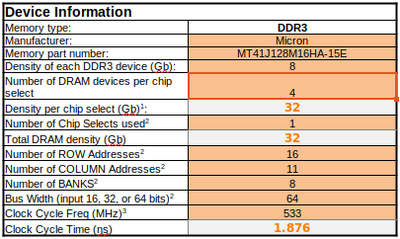
However, when we load from this XLS generated INC file to DDR Test tool, it prints the following summary:
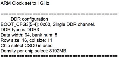
It is unclear from where this 8192MB appeared as one would expect to see 4096MB?
- 新着としてマーク
- ブックマーク
- 購読
- ミュート
- RSS フィードを購読する
- ハイライト
- 印刷
- 不適切なコンテンツを報告
Update:
It looks like that we can also successfully flash the u-boot to DDR, but GDB still fails to flash couple of chunks into DDR. This i guess is related to uncalibrated script which was generated by Register Programming Aid XLS file.
However, when running calibration with DDR Stress Test tool it hangs and i can hear USB sound detach and attach again like an indication of board reset. I do not see anything wrong in the DDR Stress Test log.
============================================
        DDR Stress Test (3.0.0)
        Build: Dec 14 2018, 14:12:06
        NXP Semiconductors.
============================================

============================================
        Chip ID
CHIP ID = i.MX6 Dual/Quad (0x63)
Internal Revision = TO1.5
============================================

============================================
        Boot Configuration
SRC_SBMR1(0x020d8004) = 0x00005870
SRC_SBMR2(0x020d801c) = 0x02000011
============================================

ARM Clock set to 1GHz

============================================
        DDR configuration
BOOT_CFG3[5-4]: 0x00, Single DDR channel.
DDR type is DDR3
Data width: 64, bank num: 8
Row size: 16, col size: 10
Chip select CSD0 is used
Density per chip select: 4096MB
============================================

Current Temperature: 45
============================================

DDR Freq: 528 MHz

ddr_mr1=0x00000000
Start write leveling calibration...
running Write level HW calibration
  MPWLHWERR register read out for factory diagnostics:
  MPWLHWERR PHY0 = 0x3c3c1e1e
  MPWLHWERR PHY1 = 0x3c3c3c78

Write leveling calibration completed, update the following registers in your initialization script
    MMDC_MPWLDECTRL0 ch0 (0x021b080c) = 0x001F001F
    MMDC_MPWLDECTRL1 ch0 (0x021b0810) = 0x00330021
    MMDC_MPWLDECTRL0 ch1 (0x021b480c) = 0x003C0046
    MMDC_MPWLDECTRL1 ch1 (0x021b4810) = 0x003A0036
Write DQS delay result:
   Write DQS0 delay: 31/256 CK
   Write DQS1 delay: 31/256 CK
   Write DQS2 delay: 33/256 CK
   Write DQS3 delay: 51/256 CK
   Write DQS4 delay: 70/256 CK
   Write DQS5 delay: 60/256 CK
Could someone suggest what might be wrong with DDR Stress Test? I have tried using the JTAG Stress Test but it never worked for me. It always stops before calibration with the following message:
Starting DQS gating calibration
. HC_DEL=0x00000000⇥    result[00]=0x11111111
. HC_DEL=0x00000001⇥    result[01]=0x11111111
. HC_DEL=0x00000002⇥    result[02]=0x11111111
. HC_DEL=0x00000003⇥    result[03]=0x11111111
. HC_DEL=0x00000004⇥    result[04]=0x11111111
. HC_DEL=0x00000005⇥    result[05]=0x11111111
. HC_DEL=0x00000006⇥    result[06]=0x11111111
. HC_DEL=0x00000007⇥    result[07]=0x11111111
. HC_DEL=0x00000008⇥    result[08]=0x11111111
. HC_DEL=0x00000009⇥    result[09]=0x11111111
. HC_DEL=0x0000000A⇥    result[0A]=0x11111111
. HC_DEL=0x0000000B⇥    result[0B]=0x11111111
. HC_DEL=0x0000000C⇥    result[0C]=0x11111111
. HC_DEL=0x0000000D⇥    result[0D]=0x11111111
ERROR FOUND, we can't get suitable value !!!!
dram test fails for all values.
Error: failed during ddr calibration
Is there a way to resolve this problem with DDR Stress Test program?
Sanket_Parekh
- 新着としてマーク
- ブックマーク
- 購読
- ミュート
- RSS フィードを購読する
- ハイライト
- 印刷
- 不適切なコンテンツを報告
Hello @davithakobyan
I hope you are doing well.
->Please make sure that all of the power connections to your DDR memory are secure.
->Please make sure that the DDR Stress Test program is compatible with your specific hardware configuration.
->Please make sure that you are using the latest version of the program. You can download the latest version from the NXP website.
->Please make sure the ARM clock is properly configured.
->Please make sure that it may be possible that there may be hardware issues with the DDR memory or other components. Check for any physical defects, loose connections, or soldering problems.
I hope this helps!
Thanks & Regards,
Sanket Parekh
- 新着としてマーク
- ブックマーク
- 購読
- ミュート
- RSS フィードを購読する
- ハイライト
- 印刷
- 不適切なコンテンツを報告
Update:
As i mentioned in the previous post i used the following configuration in XLS file of Register Programming Aid 2.4.
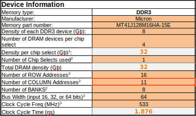
However, i could not use the generated INC file to calibrate the DDR further because the DDR Test tool hangs and from USB sound I assume that this is due to restart of attached USB controller (maybe due to restart of device). This is the log message at which DDR Test tool 3.0.0 stops:
============================================
        DDR Stress Test (3.0.0)
        Build: Dec 14 2018, 14:12:06
        NXP Semiconductors.
============================================

============================================
        Chip ID
CHIP ID = i.MX6 Dual/Quad (0x63)
Internal Revision = TO1.5
============================================

============================================
        Boot Configuration
SRC_SBMR1(0x020d8004) = 0x00005870
SRC_SBMR2(0x020d801c) = 0x02000011
============================================

ARM Clock set to 1GHz

============================================
        DDR configuration
BOOT_CFG3[5-4]: 0x00, Single DDR channel.
DDR type is DDR3
Data width: 64, bank num: 8
Row size: 16, col size: 11
Chip select CSD0 is used
Density per chip select: 8192MB
============================================

Current Temperature: 47
============================================

DDR Freq: 528 MHz

ddr_mr1=0x00000000
Start write leveling calibration...
running Write level HW calibration
  MPWLHWERR register read out for factory diagnostics:
  MPWLHWERR PHY0 = 0x3c3c1e1e
  MPWLHWERR PHY1 = 0x3c3c3c78

Write leveling calibration completed, update the following registers in your initialization script
    MMDC_MPWLDECTRL0 ch0 (0x021b080c) = 0x001F001F
    MMDC_MPWLDECTRL1 ch0 (0x021b0810) = 0x00330021
    MMDC_MPWLDECTRL0 ch1 (0x021b480c) = 0x003C0046
    MMDC_MPWLDECTRL1 ch1 (0x021b4810) = 0x003A0036
Write DQS delay result:
   Write DQS0 delay: 31/256 CK
   Write DQS1 delay: 31/256 CK
   Write DQS2 delay: 33/256 CK
   Write DQS3 delay: 51/256 CK
   Write DQS4 delay: 70/256 CK
   Write DQS5 delay: 60/256 CK
   Write DQS6 delay: 54/256 CK
As one can see the tool calculates the density per chip select as 8192 MB, but it should be 4096 MB.
We have 4 DDR chips using a single CS0 and each of which is 1 Gb (with 16 bit row, 11 bit column and 8 banks).
So the wrong density per chip which the DDT Test tool calculates may be the reason of its hanging.
Using the JTAG version of DDR Stress Test gives the following output:
Starting DQS gating calibration
. HC_DEL=0x00000000⇥	result[00]=0x11111111
. HC_DEL=0x00000001⇥	result[01]=0x11111111
. HC_DEL=0x00000002⇥	result[02]=0x11111111
. HC_DEL=0x00000003⇥	result[03]=0x11111111
. HC_DEL=0x00000004⇥	result[04]=0x11111111
. HC_DEL=0x00000005⇥	result[05]=0x11111111
. HC_DEL=0x00000006⇥	result[06]=0x11111111
. HC_DEL=0x00000007⇥	result[07]=0x11111111
. HC_DEL=0x00000008⇥	result[08]=0x11111111
. HC_DEL=0x00000009⇥	result[09]=0x11111111
. HC_DEL=0x0000000A⇥	result[0A]=0x11111111
. HC_DEL=0x0000000B⇥	result[0B]=0x11111111
. HC_DEL=0x0000000C⇥	result[0C]=0x11111111
. HC_DEL=0x0000000D⇥	result[0D]=0x11111111
ERROR FOUND, we can't get suitable value !!!!
dram test fails for all values.
Error: failed during ddr calibration
But i am inclined to think that the generated INC file is correct because when using its data for JTAG debugging, i can finally see that some chunks that are downloaded into DDR the result of the verification is OK.
So, it seems that it is simply because of uncalibrated INC file data that i use to download the u-boot binary gives for some downloaded chunks "Verify failed". Unfortunately, i cannot calibrate the DDR memory with generated INC neither with DDR Stress Test tool (for the reason already mentioned) nor with JTAG variant of DDR Test tool. Both ways fails.
Is it possible to somehow convince the DDR Stress Test GUI program to correctly calculate the DDR density?
