- Forums
- Product Forums
- General Purpose MicrocontrollersGeneral Purpose Microcontrollers
- i.MX Forumsi.MX Forums
- QorIQ Processing PlatformsQorIQ Processing Platforms
- Identification and SecurityIdentification and Security
- Power ManagementPower Management
- MCX Microcontrollers
- S32G
- S32K
- S32V
- MPC5xxx
- Other NXP Products
- Wireless Connectivity
- S12 / MagniV Microcontrollers
- Powertrain and Electrification Analog Drivers
- Sensors
- Vybrid Processors
- Digital Signal Controllers
- 8-bit Microcontrollers
- ColdFire/68K Microcontrollers and Processors
- PowerQUICC Processors
- OSBDM and TBDML
- S32M
-
- Solution Forums
- Software Forums
- MCUXpresso Software and ToolsMCUXpresso Software and Tools
- CodeWarriorCodeWarrior
- MQX Software SolutionsMQX Software Solutions
- Model-Based Design Toolbox (MBDT)Model-Based Design Toolbox (MBDT)
- FreeMASTER
- eIQ Machine Learning Software
- Embedded Software and Tools Clinic
- S32 SDK
- S32 Design Studio
- GUI Guider
- Zephyr Project
- Voice Technology
- Application Software Packs
- Secure Provisioning SDK (SPSDK)
- Processor Expert Software
- MCUXpresso Training Hub
-
- Topics
- Mobile Robotics - Drones and RoversMobile Robotics - Drones and Rovers
- NXP Training ContentNXP Training Content
- University ProgramsUniversity Programs
- Rapid IoT
- NXP Designs
- SafeAssure-Community
- OSS Security & Maintenance
- Using Our Community
-
- Cloud Lab Forums
-
- Knowledge Bases
- ARM Microcontrollers
- i.MX Processors
- Identification and Security
- Model-Based Design Toolbox (MBDT)
- QorIQ Processing Platforms
- S32 Automotive Processing Platform
- Wireless Connectivity
- CodeWarrior
- MCUXpresso Suite of Software and Tools
- MQX Software Solutions
-
Hi all
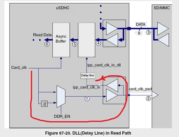
Please tell me a "DLL in read path" in uSDHC controller.
I have question about function, clock root and usage instructions.
I'm watchin Figure 67-20 in following document.
http://cache.freescale.com/files/32bit/doc/ref_manual/IMX6SDLRM.pdf
What is a function of the box that is between ④ and ⑤ ?
I can't understand their clock root because their some difference between Figure 67-2 and 67-20.
In my understandig, the clock that is shown in ① in Figure 67-20 is ref_clk.
Is it correct ?
Does it change their name to "ipp_card_clk_in" ?
According to the descrition of DLL, the DLL can be disabled or bypassed.
What is different between disabled and bypassed ?
Is the read path same that is shown in Figure 67-20 when user disabled or bypassed the DLL ?
Ko-hey
已解决! 转到解答。
Hi Yuri
Thank you for reply but I want to confirm more.
> "ipp_card_clk_in" is internal signal - from "card_clk_pad"
I can't understand that it comes from card_clk_pad.
The card_clk_pad is output, isn't it ?
Does both ipp_card_clk_in and card_clk_pad are divided from card_clk ?
> What is different between disabled and bypassed ?
I read uSDHCx_DLL_CTRL field descriptions and understand it as below.
Is it correct ?
DLL Enable = Automatically adjust ⇒ Set DLL_CTRL_SLV_OVERRIDE field to "0" and DLL_CTRL_ENABLE field to "1"
DLL Bypass = Manually adjust ⇒ Set DLL_CTRL_SLV_OVERRIDE field to "1" and DLL_CTRL_ENABLE field to "0"
DLL Disable = No adjust ⇒ Set DLL_CTRL_SLV_OVERRIDE field to "0" and DLL_CTRL_ENABLE field to "0"
Ko-hey
Hello !
Please look at my comments below.
1.
> What is a function of the box that is between ④ and ⑤ ?
This is a latch register.
2.
> In my understandig, the clock that is shown in ① in Figure 67-20 is ref_clk.
> Is it correct ?
The clock ① is a derivative of “Card_clk”, mentioned on both figures 67-20 and 67-2.
2.1.
> Does it change their name to "ipp_card_clk_in" ?
“ipp_card_clk_in” is internal signal - from “card_clk_pad” (SDx_CLK of SD interface).
3.
> What is different between disabled and bypassed ?
According to section 67.5.3.2.4 [DLL (Delay Line) in Read Path] of the RM,
“The reasons why the DLL is needed for uSDHC are 1.) the path of read data traveling
from card to host varies. 2.) in SD/MMC DDR mode the minimum input setup and hold
time are both at 2.5 ns. The data sampling window is so small that the delay of loopback
clock needs to be accurate and consistent regardless of PVT”.
The DLL is needed for high frequency cases, in particular for the DDR mode.
4.
> Is the read path same that is shown in Figure 67-20 when user disabled or bypassed the DLL ?
Basically – yes. But “ipp_card_clk_in_dll” “and ipp_card_clk_in” are the same : the “delay line”
is skipped.
Have a great day,
Yuri
-----------------------------------------------------------------------------------------------------------------------
Note: If this post answers your question, please click the Correct Answer button. Thank you!
-----------------------------------------------------------------------------------------------------------------------
Hi Yuri
Thank you for reply but I want to confirm more.
> "ipp_card_clk_in" is internal signal - from "card_clk_pad"
I can't understand that it comes from card_clk_pad.
The card_clk_pad is output, isn't it ?
Does both ipp_card_clk_in and card_clk_pad are divided from card_clk ?
> What is different between disabled and bypassed ?
I read uSDHCx_DLL_CTRL field descriptions and understand it as below.
Is it correct ?
DLL Enable = Automatically adjust ⇒ Set DLL_CTRL_SLV_OVERRIDE field to "0" and DLL_CTRL_ENABLE field to "1"
DLL Bypass = Manually adjust ⇒ Set DLL_CTRL_SLV_OVERRIDE field to "1" and DLL_CTRL_ENABLE field to "0"
DLL Disable = No adjust ⇒ Set DLL_CTRL_SLV_OVERRIDE field to "0" and DLL_CTRL_ENABLE field to "0"
Ko-hey
