- Forums
- Product Forums
- General Purpose MicrocontrollersGeneral Purpose Microcontrollers
- i.MX Forumsi.MX Forums
- QorIQ Processing PlatformsQorIQ Processing Platforms
- Identification and SecurityIdentification and Security
- Power ManagementPower Management
- MCX Microcontrollers
- S32G
- S32K
- S32V
- MPC5xxx
- Other NXP Products
- Wireless Connectivity
- S12 / MagniV Microcontrollers
- Powertrain and Electrification Analog Drivers
- Sensors
- Vybrid Processors
- Digital Signal Controllers
- 8-bit Microcontrollers
- ColdFire/68K Microcontrollers and Processors
- PowerQUICC Processors
- OSBDM and TBDML
- S32M
-
- Solution Forums
- Software Forums
- MCUXpresso Software and ToolsMCUXpresso Software and Tools
- CodeWarriorCodeWarrior
- MQX Software SolutionsMQX Software Solutions
- Model-Based Design Toolbox (MBDT)Model-Based Design Toolbox (MBDT)
- FreeMASTER
- eIQ Machine Learning Software
- Embedded Software and Tools Clinic
- S32 SDK
- S32 Design Studio
- GUI Guider
- Zephyr Project
- Voice Technology
- Application Software Packs
- Secure Provisioning SDK (SPSDK)
- Processor Expert Software
- MCUXpresso Training Hub
-
- Topics
- Mobile Robotics - Drones and RoversMobile Robotics - Drones and Rovers
- NXP Training ContentNXP Training Content
- University ProgramsUniversity Programs
- Rapid IoT
- NXP Designs
- SafeAssure-Community
- OSS Security & Maintenance
- Using Our Community
-
- Cloud Lab Forums
-
- Knowledge Bases
- ARM Microcontrollers
- i.MX Processors
- Identification and Security
- Model-Based Design Toolbox (MBDT)
- QorIQ Processing Platforms
- S32 Automotive Processing Platform
- Wireless Connectivity
- CodeWarrior
- MCUXpresso Suite of Software and Tools
- MQX Software Solutions
-
DDR3 calibration tool write leveling issue
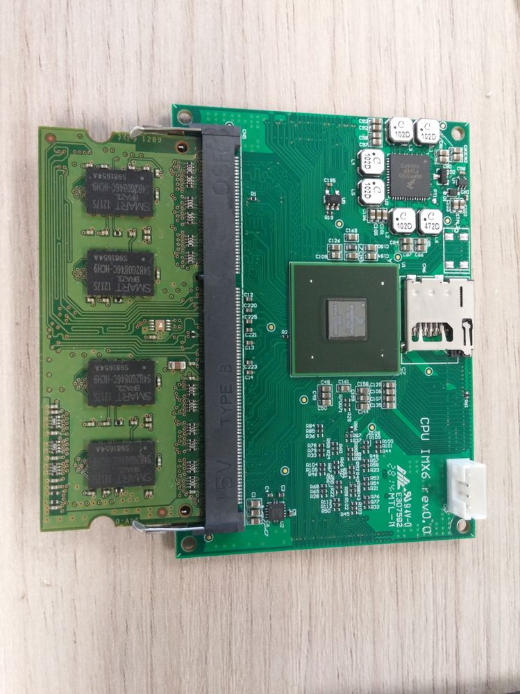
I have a custom board similar to SabreSD using latest Linux release (Yocto dizzy). I use a standard notebook memory module (204 pin SODIMM 2GB 1333MHz/1600MHz) connected to IMX6Q processor. I have tested with a memory module manufactured by SMART Modules (2GB 1333MHz) and everything works well. I have used the calibration and stress tool (1.0.3) and I got calibration data necessary to complete memory configuration with success.
I have tested another module, manufactured by Avant that uses NANYA memory chip and this module works too, but write leveling calibration procedure with this module finishes so fast and result for the four related registers are 0x001F001F.
MMDC_MPWLDECTRL0 ch0 after write level cal: 0x001F001F
MMDC_MPWLDECTRL1 ch0 after write level cal: 0x001F001F
MMDC_MPWLDECTRL0 ch1 after write level cal: 0x001F001F
MMDC_MPWLDECTRL1 ch1 after write level cal: 0x001F001F
I have tried some times and always the result is the same. For DQS calibration the results are as expected. For SMART M, the write leveling gives more realist result. I have made some tests and write leveling values that I get for SMART M works better in Avant memory than 0x001F001F result from write leveling calibration process for this module.
Someone knows the possible reason for this default value return?
Thanks,
Leonardo
Hi Leonardo
reason may be swapped DDR bit connections, as described in
AN4467 i.MX 6 Series DDR Calibration sect.11 Write Leveling
i.MX 6 Series write leveling calibration senses the LSB of each DQx byte for the write leveling feedback.
That means, bits 0, 8, 16, and 24 (as well as 32, 40, 48, and 56, when 64-bits DDR3 or dual 32-bits
LPDDR2 is used) of the DQ bus are being used. This fact should be considered during board design.
Best regards
igor
-----------------------------------------------------------------------------------------------------------------------
Note: If this post answers your question, please click the Correct Answer button. Thank you!
-----------------------------------------------------------------------------------------------------------------------
Hi Igor, the connection between my processor and SODIMM connector is not swapped. Maybe Avant DDR module can be some signal swap but if module does it they doesn't follow JEDEC, right?
I have a module from SMART M that write leveling calibration works well, than I believe that my connections are ok.
Hi Leonardo
it does not relates to jedec and
from picture is is not possible to say that, since one
needs to look at schematic. More details one can find in
sect.3.5.1 Swapping data lines IMX6DQ6SDLHDG
~igor
Unfortunately for memory module I haven't schematic, because it is a standard module sell to notebook market. The connection from processor to DDR connector I had care to maintain signals not swapped. Probably there's some signal swap in the AVANT PCB and in SMART M doesn't. Are there some way to estimate correct write leveling register value without use the calibration tool?
If DDR tests run without errors one can leave default vlaues.
Also one can check AN4467 i.MX 6 Series DDR Calibration
it gives steps for write leveling calibration. Run code with jtag
and choose best option experimentally.
One can look at overview of DDR Stress Test Tool
https://community.freescale.com/docs/DOC-101708
~igor
