- Forums
- Product Forums
- General Purpose MicrocontrollersGeneral Purpose Microcontrollers
- i.MX Forumsi.MX Forums
- QorIQ Processing PlatformsQorIQ Processing Platforms
- Identification and SecurityIdentification and Security
- Power ManagementPower Management
- Wireless ConnectivityWireless Connectivity
- RFID / NFCRFID / NFC
- Advanced AnalogAdvanced Analog
- MCX Microcontrollers
- S32G
- S32K
- S32V
- MPC5xxx
- Other NXP Products
- S12 / MagniV Microcontrollers
- Powertrain and Electrification Analog Drivers
- Sensors
- Vybrid Processors
- Digital Signal Controllers
- 8-bit Microcontrollers
- ColdFire/68K Microcontrollers and Processors
- PowerQUICC Processors
- OSBDM and TBDML
- S32M
- S32Z/E
-
- Solution Forums
- Software Forums
- MCUXpresso Software and ToolsMCUXpresso Software and Tools
- CodeWarriorCodeWarrior
- MQX Software SolutionsMQX Software Solutions
- Model-Based Design Toolbox (MBDT)Model-Based Design Toolbox (MBDT)
- FreeMASTER
- eIQ Machine Learning Software
- Embedded Software and Tools Clinic
- S32 SDK
- S32 Design Studio
- GUI Guider
- Zephyr Project
- Voice Technology
- Application Software Packs
- Secure Provisioning SDK (SPSDK)
- Processor Expert Software
- Generative AI & LLMs
-
- Topics
- Mobile Robotics - Drones and RoversMobile Robotics - Drones and Rovers
- NXP Training ContentNXP Training Content
- University ProgramsUniversity Programs
- Rapid IoT
- NXP Designs
- SafeAssure-Community
- OSS Security & Maintenance
- Using Our Community
-
- Cloud Lab Forums
-
- Knowledge Bases
- ARM Microcontrollers
- i.MX Processors
- Identification and Security
- Model-Based Design Toolbox (MBDT)
- QorIQ Processing Platforms
- S32 Automotive Processing Platform
- Wireless Connectivity
- CodeWarrior
- MCUXpresso Suite of Software and Tools
- MQX Software Solutions
- RFID / NFC
- Advanced Analog
-
- NXP Tech Blogs
- Home
- :
- 无线连接
- :
- Wireless MCU
- :
- Using QN908x Development kit to program external QN9080 device
Using QN908x Development kit to program external QN9080 device
Using QN908x Development kit to program external QN9080 device
Dear experts,
When making a QN9080 application system, I understand that the "external target debug interface" on the QN9080-DK board can be used for the debugging of the external device.

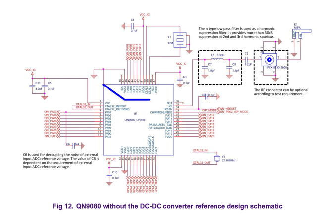
And there are quite many ports on the external target debug interface, mostly for SWD and JTAG communication. I will connect pin 2 and pin 4 of the interface to PA22 and PA23 of the external QN908x, and the ISPEN (pin 9) to pin 33 (CHIPMODE/PB02) of the external device.
And, should I leave the other pins (pin 1, 6, 8, 9, 10 of the external target debug interface) as floating pins?
What is the role of pin 1 (connected to somewhere invisible), and pin 6 (if_detect)?
Thank you for reading it.
Best regards, DY.
Hi @DeeY,
In order to program an off-board target, these jumper configurations are needed (Section 3.1.2 CMSIS-DAP to off-board target, QN908x DK User Guide
Pin 1 is connected to VCC depending on JP2 configuration:
Pin 9 (IF_DETECTED) is connected directly into LPC4322:
This schematic is located in QN9080DK's page, in the section of Design Resources (Design files for QN9080-DK).
As for design and connections, please help me looking into Design Considerations for Debug. I hope you find this helpful!
Best regards,
Julián


