- Forums
- Product Forums
- General Purpose MicrocontrollersGeneral Purpose Microcontrollers
- i.MX Forumsi.MX Forums
- QorIQ Processing PlatformsQorIQ Processing Platforms
- Identification and SecurityIdentification and Security
- Power ManagementPower Management
- MCX Microcontrollers
- S32G
- S32K
- S32V
- MPC5xxx
- Other NXP Products
- Wireless Connectivity
- S12 / MagniV Microcontrollers
- Powertrain and Electrification Analog Drivers
- Sensors
- Vybrid Processors
- Digital Signal Controllers
- 8-bit Microcontrollers
- ColdFire/68K Microcontrollers and Processors
- PowerQUICC Processors
- OSBDM and TBDML
- S32M
-
- Solution Forums
- Software Forums
- MCUXpresso Software and ToolsMCUXpresso Software and Tools
- CodeWarriorCodeWarrior
- MQX Software SolutionsMQX Software Solutions
- Model-Based Design Toolbox (MBDT)Model-Based Design Toolbox (MBDT)
- FreeMASTER
- eIQ Machine Learning Software
- Embedded Software and Tools Clinic
- S32 SDK
- S32 Design Studio
- GUI Guider
- Zephyr Project
- Voice Technology
- Application Software Packs
- Secure Provisioning SDK (SPSDK)
- Processor Expert Software
- MCUXpresso Training Hub
-
- Topics
- Mobile Robotics - Drones and RoversMobile Robotics - Drones and Rovers
- NXP Training ContentNXP Training Content
- University ProgramsUniversity Programs
- Rapid IoT
- NXP Designs
- SafeAssure-Community
- OSS Security & Maintenance
- Using Our Community
-
- Cloud Lab Forums
-
- Knowledge Bases
- ARM Microcontrollers
- i.MX Processors
- Identification and Security
- Model-Based Design Toolbox (MBDT)
- QorIQ Processing Platforms
- S32 Automotive Processing Platform
- Wireless Connectivity
- CodeWarrior
- MCUXpresso Suite of Software and Tools
- MQX Software Solutions
-
Hello,
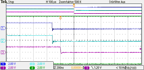
we have a T2081 board with a FPGA connected via IFC_CS2_B (normal GPCM mode). The read and write accesses should be terminated by the FPGA via transfer acknowledge signal. Unluckily every access to/from the FPGA hangs and is never terminated. I can see that the CPU begins the access by asserting CS and OE. The FPGA answers by asserting the TA signal but CPU never deasserts CS/OE. Also the timeout (IFC_CSOR2_GPCM[GPTO]) does not end the access.
=> md ffd00000
ffd00000:
(CPU HANGS)
IFC_CS2_B=dark blue IFC_OE_B=light blue IFC_RB0_B(TA)=pink
 /* DDU */
#define DDU_BASE            0xffd00000
#define DDU_BASE_PHYS        (0xf00000000ull | DDU_BASE)

#define CONFIG_SYS_CSPR2_EXT    (0xf)
#define CONFIG_SYS_CSPR2    (CSPR_PHYS_ADDR(DDU_BASE_PHYS) \
                | CSPR_PORT_SIZE_16 \
                | CSPR_MSEL_GPCM \
                | CSPR_V)
#define CONFIG_SYS_AMASK2    IFC_AMASK(1*1024*1024)
#define CONFIG_SYS_CSOR2    (CSOR_GPCM_GPTO(128*1024) \
                | CSOR_GPCM_RGETA_EXT | CSOR_GPCM_WGETA_EXT | CSOR_GPCM_BCTLD)

/* DDU Timing parameters for IFC CS2 */
#define CONFIG_SYS_CS2_FTIM0        (FTIM0_GPCM_TACSE(0x1) | \
                    FTIM0_GPCM_TEADC(0x02) | \
                    FTIM0_GPCM_TEAHC(0x01))
#define CONFIG_SYS_CS2_FTIM1        (FTIM1_GPCM_TACO(0x1) | \
                    FTIM1_GPCM_TRAD(0x1))
#define CONFIG_SYS_CS2_FTIM2        (FTIM2_GPCM_TCS(0x1) | \
                    FTIM2_GPCM_TCH(0x1) | \
                    FTIM2_GPCM_TWP(0x1))
#define CONFIG_SYS_CS2_FTIM3        0x1
I'm a little bit confused about figure 13-4 "Internal connectivity of RB signal for 28-bit address mode" in T2080RM (02/2016). First of all I think this should be called "32-bit address mode"?
I'm also a little bit unsure how to set the address mode. Does this refer to the NOR Flash strapping options (cfg_rcw_src[6:7])?
So setting cfg_rcw_src[6:7]=11 means that I have to use IFC_RB0 as acknowledge pin for every chip select (except CS1), right?
Original Attachment has been moved to: ifc_debug_details.txt.zip
已解决! 转到解答。
> First of all I think this should be called "32-bit address mode"?
Correct, this is a typo in the RM.
> I'm also a little bit unsure how to set the address mode.
> Does this refer to the NOR Flash strapping options (cfg_rcw_src[6:7])?
Please refer to the RM descriptions of IFC_GRP_A_BASE and IFC_GRP_B_BASE RCW fields.
Please note that it is reasonable to investigate this issue as a Technical Case:

