
- Forums
- Product Forums
- General Purpose MicrocontrollersGeneral Purpose Microcontrollers
- i.MX Forumsi.MX Forums
- QorIQ Processing PlatformsQorIQ Processing Platforms
- Identification and SecurityIdentification and Security
- Power ManagementPower Management
- Wireless ConnectivityWireless Connectivity
- RFID / NFCRFID / NFC
- Advanced AnalogAdvanced Analog
- Neural Processing UnitsNeural Processing Units
- MCX Microcontrollers
- S32G
- S32K
- S32V
- MPC5xxx
- Other NXP Products
- S12 / MagniV Microcontrollers
- Powertrain and Electrification Analog Drivers
- Sensors
- Vybrid Processors
- Digital Signal Controllers
- 8-bit Microcontrollers
- ColdFire/68K Microcontrollers and Processors
- PowerQUICC Processors
- OSBDM and TBDML
- S32M
- S32Z/E
-
- Solution Forums
- Software Forums
- MCUXpresso Software and ToolsMCUXpresso Software and Tools
- CodeWarriorCodeWarrior
- MQX Software SolutionsMQX Software Solutions
- Model-Based Design Toolbox (MBDT)Model-Based Design Toolbox (MBDT)
- FreeMASTER
- eIQ Machine Learning Software
- Embedded Software and Tools Clinic
- S32 SDK
- S32 Design Studio
- GUI Guider
- Zephyr Project
- Voice Technology
- Application Software Packs
- Secure Provisioning SDK (SPSDK)
- Processor Expert Software
- Generative AI & LLMs
-
- Topics
- Mobile Robotics - Drones and RoversMobile Robotics - Drones and Rovers
- NXP Training ContentNXP Training Content
- University ProgramsUniversity Programs
- Rapid IoT
- NXP Designs
- SafeAssure-Community
- OSS Security & Maintenance
- Using Our Community
-
- Cloud Lab Forums
-
- Knowledge Bases
- ARM Microcontrollers
- i.MX Processors
- Identification and Security
- Model-Based Design Toolbox (MBDT)
- QorIQ Processing Platforms
- S32 Automotive Processing Platform
- Wireless Connectivity
- CodeWarrior
- MCUXpresso Suite of Software and Tools
- MQX Software Solutions
- RFID / NFC
- Advanced Analog
- Neural Processing Units
-
- NXP Tech Blogs
- Home
- :
- QorIQプロセッシングプラットフォーム
- :
- Tシリーズ
- :
- DDR4 configuration fail - ACE Error
DDR4 configuration fail - ACE Error
- RSS フィードを購読する
- トピックを新着としてマーク
- トピックを既読としてマーク
- このトピックを現在のユーザーにフロートします
- ブックマーク
- 購読
- ミュート
- 印刷用ページ
DDR4 configuration fail - ACE Error
- 新着としてマーク
- ブックマーク
- 購読
- ミュート
- RSS フィードを購読する
- ハイライト
- 印刷
- 不適切なコンテンツを報告
I am trying to configure DDR4 (MT40A256M16 - 5 discrete devices, one is for ECC) with T1022 processor using Lauterbach probe and the registers configuration generated by Codewarrior-QCVS
Codewarrior Version: 10.5.1.
QCVS Version 4.5.0
How I do that:
- Configure DDR4 on Codewarrior-QCVS.
- Generate code.
- Translate .tcl script generated by Codewarrior-QCVS to Lautebach PRACTICE script.
- Run Lauterbach script which detect the processor, configure the RCW, configure the UART and print to the console and configure the DDR4 Controller.
- I check that all registers are configured on the processor.
Once the registers are set in the DDR4 Controller and bit MEM_EN is set, DDR Error ACE turns on as you can see in the screenshot (TRACE_32-regs.jpg) attached. I know that the ACE bit means an error in the training process.
Also you can see some of the debug registers in the screenshot.
Q1: I would like to know why it is failing and if the DEBUG registers can give us more information. Could you provide that information?
In addition you can find attached the RCW (PBL.pbl) and the DDR register configuration (ddrCtrl_1.tcl).
I also tried without success:
- Reduce the clk freq from 800MHz to 650MHz
- Measurement of 1V2 and 0V6 voltage are OK.
- Check termination of MDICx signals are OK.
- Check clk presence OK.
Q2: Is there any example code to configure DDR4 available? It could be C code, I have uboot running, but failing when it reach the DDR configuration because is trying to read SPD.
Any help will be really appreciated.
Thank you.
- 新着としてマーク
- ブックマーク
- 購読
- ミュート
- RSS フィードを購読する
- ハイライト
- 印刷
- 不適切なコンテンツを報告
1) You wrote:
> Configure DDR4 on Codewarrior-QCVS
Which exactly parameters you have specified for the QCVS DDR Tool to obtain the registers settings?
Please provide screenshot of the filled DDR configuration pane (see attached).
2) Please provide the processor connection schematics as searchable PDF for inspection and Excel table containing PCB traces lengths for all signals of the DDR interface.
- 新着としてマーク
- ブックマーク
- 購読
- ミュート
- RSS フィードを購読する
- ハイライト
- 印刷
- 不適切なコンテンツを報告
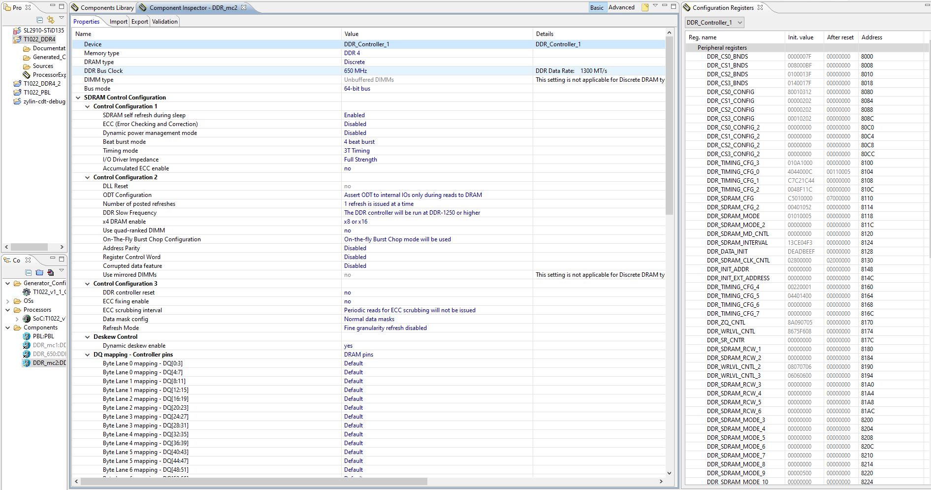
Hi
Please find attached the QCVS configuration screenshots.
Note that the initial configuration was for 1600MT/s and ECC enable, after it didn't work, those parameters were modified from QCVS.
Regarding the track distances you can find the info in the spreadsheet attached.
I need to ask for schematics approval in order to post them here, it will come later.
- 新着としてマーク
- ブックマーク
- 購読
- ミュート
- RSS フィードを購読する
- ハイライト
- 印刷
- 不適切なコンテンツを報告
Concerning provided Excel table - it does not contain the requested data.
Please provide a table containing lengths of ALL PCB traces lengths of the DDR interface signals - i.e. address/control/data.
- 新着としてマーク
- ブックマーク
- 購読
- ミュート
- RSS フィードを購読する
- ハイライト
- 印刷
- 不適切なコンテンツを報告
Hi ufedor,
Attached you can find the PCB length updated.
For Addr/ctrl i have provided the length of the signal to the first chip (U6). If you also need the lengths between the chips it gets a bit tricky, but it is about 11-12mm for all the lines varying with layer.
Your assistance is really appreciated.
Thanks
- 新着としてマーク
- ブックマーク
- 購読
- ミュート
- RSS フィードを購読する
- ハイライト
- 印刷
- 不適切なコンテンツを報告
You wrote:
> If you also need the lengths between the chips it gets a bit tricky
Excuse me, how in this case you filled numbers into the DDR Configuration "DDR4+config+real+tracks.jpg"?
What are MCK segments lengths?