
- Forums
- Product Forums
- General Purpose MicrocontrollersGeneral Purpose Microcontrollers
- i.MX Forumsi.MX Forums
- QorIQ Processing PlatformsQorIQ Processing Platforms
- Identification and SecurityIdentification and Security
- Power ManagementPower Management
- Wireless ConnectivityWireless Connectivity
- RFID / NFCRFID / NFC
- Advanced AnalogAdvanced Analog
- Neural Processing UnitsNeural Processing Units
- MCX Microcontrollers
- S32G
- S32K
- S32V
- MPC5xxx
- Other NXP Products
- S12 / MagniV Microcontrollers
- Powertrain and Electrification Analog Drivers
- Sensors
- Vybrid Processors
- Digital Signal Controllers
- 8-bit Microcontrollers
- ColdFire/68K Microcontrollers and Processors
- PowerQUICC Processors
- OSBDM and TBDML
- S32M
- S32Z/E
-
- Solution Forums
- Software Forums
- MCUXpresso Software and ToolsMCUXpresso Software and Tools
- CodeWarriorCodeWarrior
- MQX Software SolutionsMQX Software Solutions
- Model-Based Design Toolbox (MBDT)Model-Based Design Toolbox (MBDT)
- FreeMASTER
- eIQ Machine Learning Software
- Embedded Software and Tools Clinic
- S32 SDK
- S32 Design Studio
- GUI Guider
- Zephyr Project
- Voice Technology
- Application Software Packs
- Secure Provisioning SDK (SPSDK)
- Processor Expert Software
- Generative AI & LLMs
-
- Topics
- Mobile Robotics - Drones and RoversMobile Robotics - Drones and Rovers
- NXP Training ContentNXP Training Content
- University ProgramsUniversity Programs
- Rapid IoT
- NXP Designs
- SafeAssure-Community
- OSS Security & Maintenance
- Using Our Community
-
- Cloud Lab Forums
-
- Knowledge Bases
- ARM Microcontrollers
- i.MX Processors
- Identification and Security
- Model-Based Design Toolbox (MBDT)
- QorIQ Processing Platforms
- S32 Automotive Processing Platform
- Wireless Connectivity
- CodeWarrior
- MCUXpresso Suite of Software and Tools
- MQX Software Solutions
- RFID / NFC
- Advanced Analog
- Neural Processing Units
-
- NXP Tech Blogs
CPLD in RFDB T1042

Hi!
I am using T1042 and designing a board using reference board of T1042. I am using 4 flashes and they are directly connected to IFC in my board and IFC is sending control signal to CS,WE and all other signals. But in reference design board, CPLD is controlling all the control pins of Flashes. Please tell me if it is necessary to add CPLD in my board and control my flashes through CPLD
Thank You


As i am getting help from reference schematic.
1) I cannot understand the purpose of XOR gate with MSB of Flash addresses and CPLD output.
2) Also CPLD getting IFC DATA but not IFC's adress accept few pins.
Please explain my these two questions
Thank You
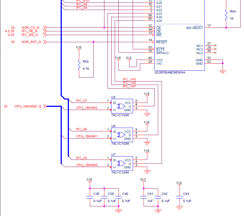
1) This is to implement "virtual banks" in the NOR Flash.
For example the CFG_VBANK0 physically swaps halves of the Flash, so it is possible to have two bootable images - main and reserved.
2) I believe that your question is connected with implementation of internal CPLD registers.
1) Is it necessary to keep two bootable images?
2) Yes, can you please explain some logic that what CPLD is doing with IFC data.
ok. i am on the final stage of my board designing. just inform me that what controls can i give to CPLD relating to flashes that IFC can not perform. If no need for CPLD to interface NOR with IFC then please inform me so that i can finalize my design.
Thank you
