- Forums
- Product Forums
- General Purpose MicrocontrollersGeneral Purpose Microcontrollers
- i.MX Forumsi.MX Forums
- QorIQ Processing PlatformsQorIQ Processing Platforms
- Identification and SecurityIdentification and Security
- Power ManagementPower Management
- Wireless ConnectivityWireless Connectivity
- RFID / NFCRFID / NFC
- MCX Microcontrollers
- S32G
- S32K
- S32V
- MPC5xxx
- Other NXP Products
- S12 / MagniV Microcontrollers
- Powertrain and Electrification Analog Drivers
- Sensors
- Vybrid Processors
- Digital Signal Controllers
- 8-bit Microcontrollers
- ColdFire/68K Microcontrollers and Processors
- PowerQUICC Processors
- OSBDM and TBDML
- S32M
-
- Solution Forums
- Software Forums
- MCUXpresso Software and ToolsMCUXpresso Software and Tools
- CodeWarriorCodeWarrior
- MQX Software SolutionsMQX Software Solutions
- Model-Based Design Toolbox (MBDT)Model-Based Design Toolbox (MBDT)
- FreeMASTER
- eIQ Machine Learning Software
- Embedded Software and Tools Clinic
- S32 SDK
- S32 Design Studio
- GUI Guider
- Zephyr Project
- Voice Technology
- Application Software Packs
- Secure Provisioning SDK (SPSDK)
- Processor Expert Software
-
- Topics
- Mobile Robotics - Drones and RoversMobile Robotics - Drones and Rovers
- NXP Training ContentNXP Training Content
- University ProgramsUniversity Programs
- Rapid IoT
- NXP Designs
- SafeAssure-Community
- OSS Security & Maintenance
- Using Our Community
-
- Cloud Lab Forums
-
- Knowledge Bases
- ARM Microcontrollers
- i.MX Processors
- Identification and Security
- Model-Based Design Toolbox (MBDT)
- QorIQ Processing Platforms
- S32 Automotive Processing Platform
- Wireless Connectivity
- CodeWarrior
- MCUXpresso Suite of Software and Tools
- MQX Software Solutions
- RFID / NFC
-
Unbricking S32K146
Hello,
I've got a development board with S32K146 which seems to be somehow corrupted. It worked correctly some time ago, but now I cannot reprogram it with S32 Design Studio for ARM. The result under S32DS is like this:
and it is not possible to program the MCU - because after click on Retry this window appear again and again.
I suspect that something went wrong when I tried to program the MCU with copying some .srec file using Mass Storage programming method.
I can see this board as a Mass Storage device under my Linux system, but I'm not sure if there is everything ok with the partitions presented on it:
# fdisk -l
Disk /dev/sdb: 968.8 MiB, 1015807488 bytes, 1983999 sectors
Disk model: FSL/PEMICRO MSD
Units: sectors of 1 * 512 = 512 bytes
Sector size (logical/physical): 512 bytes / 512 bytes
I/O size (minimum/optimal): 512 bytes / 512 bytes
Disklabel type: dos
Disk identifier: 0x0001022b
Device Boot Start End Sectors Size Id Type
/dev/sdb1 2048 249855 247808 121M 6 FAT16
The suspected in following dump are size of the disk (968.8 MiB) and the partition size (121M).
I tried to repair this board with Kinetis Recovery Utility under Windows but it showed the message that it is still trying to halt the processor and I should replug power supply. I replugged usb connector but the Kinetis Recovery Utility still shows this message.
I've seen somewhere that there are some partitions on the flash memory. Maybe this partitions are corrupted?
I've got Segger J-Link debugger also - maybe with it I could repair the board somehow?
Hello,
Please scope the reset pin, is it in reset? Have you measured VDD voltage?
Have you tried loading an application using the J-link debugger from the S32DS?
If not, please try to load an SDK example.
Thank you,
Daniel
I didn't test the reset pin nor Vdd voltage yet, but D1 led (red one) is continuously turned on.
J-Link debugger cannot connect to this MCU - even it can't recognize the MCU. The screenshot I attached in my first post is taken when I tried to load application from S32DS via OpenSDA.
I'm afraid I secured permanently the MCU because I've made some mistake in my linker script and probably the area 0x400-0x40f has been overwritten by binary code. So everything could be placed there.
Seems like the only option is to solder new MCU now? Am I right?
Hi,
Could you please try to read the MDM_AP status and control registers first.
Use J-link commander and these commands:
J-Link>r0 // pull reset pin low
J-Link>swdwritedp 2,0x01000000 // MDM_AP status register
J-Link>swdreadap 0 // Read MDM_AP status register
J-Link>swdreadap 0 // Read MDM_AP status register (has to be done 2x) Flash memory ready and Mass erase enable bits should be set
J-Link>swdreadap 1 // Read MDM_AP control register
J-Link>swdreadap 1 // Read MDM_AP control register (has to be done 2x)
J-Link>unlock Kinetis // Erase and unsecure the MCU
For more information about the register please refer to Section 56.6 MDM-AP status and control registers, RM rev.9.
You should be able to see if the MCU secured (Status[2]), if the Mass Erase operation is enabled (Status[5]) and if the Flash memory is ready (Status[1]).
Thank you,
BR, Daniel
I cannot connect to the target MCU, because:
-----begin----
/usr/local/JLink_Linux_V644g_x86_64_orig/JLinkExe
SEGGER J-Link Commander V6.44g (Compiled Apr 18 2019 17:15:12)
DLL version V6.44g, compiled Apr 18 2019 17:15:02
Connecting to J-Link via USB...O.K.
Firmware: J-Link Ultra V4 compiled May 27 2019 15:49:24
Hardware version: V4.00
S/N: 504501625
License(s): RDI, FlashBP, FlashDL, JFlash, GDB
VTref=3.300V (fixed)
Type "connect" to establish a target connection, '?' for help
J-Link>connect
Please specify device / core. <Default>: S32K146 (ALLOW SECURITY)
Type '?' for selection dialog
Device>S32K146
Please specify target interface:
J) JTAG (Default)
S) SWD
T) cJTAG
TIF>S
Specify target interface speed [kHz]. <Default>: 4000 kHz
Speed>4000
Device "S32K146" selected.
Connecting to target via SWD
InitTarget()
Protection bytes in flash at addr. 0x400 - 0x40F indicate that readout protection is set.
For debugger connection the device needs to be unsecured.
Note: Unsecuring will trigger a mass erase of the internal flash.
Device will be unsecured now.
Timeout while unsecuring device. Erase never stops.
Found SW-DP with ID 0x2BA01477
Scanning AP map to find all available APs
AP[2]: Stopped AP scan as end of AP map has been reached
AP[0]: AHB-AP (IDR: 0x24770011)
AP[1]: JTAG-AP (IDR: 0x001C0000)
Iterating through AP map to find AHB-AP to use
AP[0]: Skipped. Invalid implementer code read from CPUIDVal[31:24] = 0x00
AP[1]: Skipped. Not an AHB-AP
****** Error: Could not find core in Coresight setup
InitTarget()
Protection bytes in flash at addr. 0x400 - 0x40F indicate that readout protection is set.
For debugger connection the device needs to be unsecured.
Note: Unsecuring will trigger a mass erase of the internal flash.
Device will be unsecured now.
Timeout while unsecuring device. Erase never stops.
Found SW-DP with ID 0x2BA01477
Scanning AP map to find all available APs
AP[2]: Stopped AP scan as end of AP map has been reached
AP[0]: AHB-AP (IDR: 0x24770011)
AP[1]: JTAG-AP (IDR: 0x001C0000)
Iterating through AP map to find AHB-AP to use
AP[0]: Skipped. Invalid implementer code read from CPUIDVal[31:24] = 0x00
AP[1]: Skipped. Not an AHB-AP
Cannot connect to target.
J-Link>
----end----
When I try to run your commands I've got following error:
J-Link>r0
J-Link>swdwritedp 2,0x01000000
****** Error: Communication timed out: Requested 4 bytes, received 0 bytes !
Write DP register 2 = 0x01000000 ***ERROR
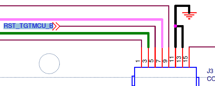
Probably a long shot, but can you hold the reset pin low externally (J3.5 - J3.11) and try with the J-link commander, then release the pin and check again?
Thank you,
BR, Daniel
Hello Daniel,
Thank you for your suggestions.
I've made the connection between J3.5-J3.11 - as you proposed and now it is possible to issue some commands under Jlink commander:
J-Link>R0
J-Link>swdwritedp 2,0x01000000
Write DP register 2 = 0x01000000
J-Link>swdreadap 0
Read AP register 0 = 0x00000000
J-Link>swdreadap 0
Read AP register 0 = 0x00000034
J-Link>swdreadap 1
Read AP register 1 = 0x00000034
J-Link>swdreadap 1
Read AP register 1 = 0x00000001
J-Link>swdwriteap 1,0x1
Write AP register 1 = 0x00000001
If I interpret the registers correctly the status reg has set following bits (0x34):
2 - system security
4 - reserved
5 - mass erase enable
and the control reg (0x1):
0 - flash memory mass erase in progress
Whan can I do next?
Hi Witold,
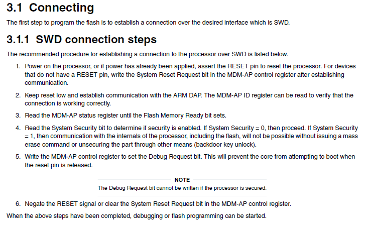
These are the SWD connection steps described in AN12130 Production Flash Programming Best Practices for S32K1xx MCUs.
In this case, however, the Flash Ready bit (Status[1]) is not set and the mass erase operation (control[0]) can't complete for some reason. I don't think there is a solution other than replacing the MCU, unfortunately.
BR, Daniel


