- Forums
- Product Forums
- General Purpose MicrocontrollersGeneral Purpose Microcontrollers
- i.MX Forumsi.MX Forums
- QorIQ Processing PlatformsQorIQ Processing Platforms
- Identification and SecurityIdentification and Security
- Power ManagementPower Management
- Wireless ConnectivityWireless Connectivity
- RFID / NFCRFID / NFC
- Advanced AnalogAdvanced Analog
- MCX Microcontrollers
- S32G
- S32K
- S32V
- MPC5xxx
- Other NXP Products
- S12 / MagniV Microcontrollers
- Powertrain and Electrification Analog Drivers
- Sensors
- Vybrid Processors
- Digital Signal Controllers
- 8-bit Microcontrollers
- ColdFire/68K Microcontrollers and Processors
- PowerQUICC Processors
- OSBDM and TBDML
- S32M
- S32Z/E
-
- Solution Forums
- Software Forums
- MCUXpresso Software and ToolsMCUXpresso Software and Tools
- CodeWarriorCodeWarrior
- MQX Software SolutionsMQX Software Solutions
- Model-Based Design Toolbox (MBDT)Model-Based Design Toolbox (MBDT)
- FreeMASTER
- eIQ Machine Learning Software
- Embedded Software and Tools Clinic
- S32 SDK
- S32 Design Studio
- GUI Guider
- Zephyr Project
- Voice Technology
- Application Software Packs
- Secure Provisioning SDK (SPSDK)
- Processor Expert Software
- Generative AI & LLMs
-
- Topics
- Mobile Robotics - Drones and RoversMobile Robotics - Drones and Rovers
- NXP Training ContentNXP Training Content
- University ProgramsUniversity Programs
- Rapid IoT
- NXP Designs
- SafeAssure-Community
- OSS Security & Maintenance
- Using Our Community
-
- Cloud Lab Forums
-
- Knowledge Bases
- ARM Microcontrollers
- i.MX Processors
- Identification and Security
- Model-Based Design Toolbox (MBDT)
- QorIQ Processing Platforms
- S32 Automotive Processing Platform
- Wireless Connectivity
- CodeWarrior
- MCUXpresso Suite of Software and Tools
- MQX Software Solutions
- RFID / NFC
- Advanced Analog
-
- NXP Tech Blogs
in file S32K3_SPD_BIST_UM.pdf,Mentioned "Main reset domain (RD0)",
Table 3-[1],S32K3xx Reference Manual,I didn't find a full explanation about "Main reset domain (RD0)"
I would like the NXP team to help explain what Main reset domain (RD0) means.
Looking forward to your reply, thank you very much.
已解决! 转到解答。
Hello,
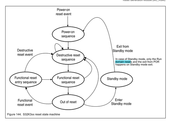
Not sure what do you mean by main reset. Looking at reference manual, it seems to me that main reset is term taken from devices that apply multiple reset domains. So its just a general term and here it will mean the reset domain, as here is only one.
But Reset generation module embed:
So there are only these in so called "main domain":
• Chip reset sequences
— POR
— Destructive reset
— Functional reset
Best regards,
Peter
Hello,
Main reset domain is the reset state of the device for K3. S32K3 has just one.
So the more complex devices, has more reset domains, but this is not the case of S32K3.
Best regards,
Peter
Thanks for your reply
“Main reset domain is the reset state of the device for K3. S32K3 has just one”
I want to know What is the relationship between main reset and destructive reset and functional reset and POR?
Hello,
Not sure what do you mean by main reset. Looking at reference manual, it seems to me that main reset is term taken from devices that apply multiple reset domains. So its just a general term and here it will mean the reset domain, as here is only one.
But Reset generation module embed:
So there are only these in so called "main domain":
• Chip reset sequences
— POR
— Destructive reset
— Functional reset
Best regards,
Peter


