- Forums
- Product Forums
- General Purpose MicrocontrollersGeneral Purpose Microcontrollers
- i.MX Forumsi.MX Forums
- QorIQ Processing PlatformsQorIQ Processing Platforms
- Identification and SecurityIdentification and Security
- Power ManagementPower Management
- Wireless ConnectivityWireless Connectivity
- RFID / NFCRFID / NFC
- MCX Microcontrollers
- S32G
- S32K
- S32V
- MPC5xxx
- Other NXP Products
- S12 / MagniV Microcontrollers
- Powertrain and Electrification Analog Drivers
- Sensors
- Vybrid Processors
- Digital Signal Controllers
- 8-bit Microcontrollers
- ColdFire/68K Microcontrollers and Processors
- PowerQUICC Processors
- OSBDM and TBDML
- S32M
-
- Solution Forums
- Software Forums
- MCUXpresso Software and ToolsMCUXpresso Software and Tools
- CodeWarriorCodeWarrior
- MQX Software SolutionsMQX Software Solutions
- Model-Based Design Toolbox (MBDT)Model-Based Design Toolbox (MBDT)
- FreeMASTER
- eIQ Machine Learning Software
- Embedded Software and Tools Clinic
- S32 SDK
- S32 Design Studio
- GUI Guider
- Zephyr Project
- Voice Technology
- Application Software Packs
- Secure Provisioning SDK (SPSDK)
- Processor Expert Software
-
- Topics
- Mobile Robotics - Drones and RoversMobile Robotics - Drones and Rovers
- NXP Training ContentNXP Training Content
- University ProgramsUniversity Programs
- Rapid IoT
- NXP Designs
- SafeAssure-Community
- OSS Security & Maintenance
- Using Our Community
-
- Cloud Lab Forums
-
- Knowledge Bases
- ARM Microcontrollers
- i.MX Processors
- Identification and Security
- Model-Based Design Toolbox (MBDT)
- QorIQ Processing Platforms
- S32 Automotive Processing Platform
- Wireless Connectivity
- CodeWarrior
- MCUXpresso Suite of Software and Tools
- MQX Software Solutions
-
How can I define variable in S32K146 RAM_U
Hi everyone,
when i define a array more than 64KB (or two with 32KB),
the compiler said m_data_2 overflowed.
but In S32K146 ,there are RAM_L(64KB) and RAM_U(64KB) , totally 128KB , so How can I define variable in S32K146 RAM_U?
thanks a lot
Hi Willian,
At first, I would like to mention that SRAM_U has a size of 60 KB. That is why you have had difficulties with placing two 32 KB arrays into the m_data_2 section.
You can refer to RM rev 12.1
There are two regions:
- SRAM_L from 1FFF_0000h to 1FFF_FFFFh
- SRAM_U from 2000_0000h to 2000_EFFFh
There is an important note:
"Misaligned accesses across the 2000_0000h boundary are not
supported in the Arm Cortex-M4F architecture"
So, that is why it is easier to have two RAM segments in the linker file.
Also, I suggest you to look at the linker file of the project to see what else is placed in the m_data/ m_data_2 sections (heap, stack).
Best regards,
Diana
Hi Ahmad,
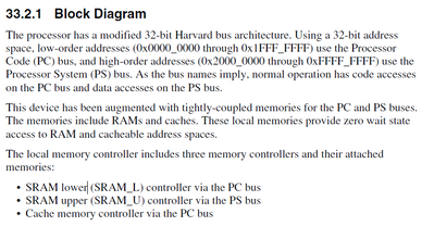
At first, I would like to suggest looking at RM rev 12.1 section 33.2.1. Each region uses a different bus:
When you look at the linker file of some project, you can see that SRAM_L (m_data) includes the code_ram section, global variables, vector table. SRAM_U (m_data_2) contains stack and heap.
The benefit of this approach is described in the AN below in the section "3.1 SRAM accesses"
https://www.nxp.com/docs/en/application-note/AN4745.pdf
"The dual SRAM blocks allow the SRAM controller to handle simultaneous accesses to the SRAMs as long as
those accesses are not to the same SRAM block. Allowable simultaneous accesses to the SRAM are:
• Core CODE (SRAM_L) and core system (SRAM_U) accesses
• Core CODE (SRAM_L) and non-core master to SRAM_U
• Core system (SRAM_U) and non-core master to SRAM_L
Strategic placement of code and data into each of the SRAM blocks can help to increase parallelism and overall performance.
For a typical application, placing critical code in the SRAM_L block and placing data and the stack into the SRAM_U block
will yield the best performance."
Best regards,
Diana
thanks for your kind reply.
what is main difference between CODE BUS & SYSTEM BUS? (both of them come from CPU?)
and what can be "critical code" ?
Hi,
I assume that your question is already answered here:
https://community.nxp.com/t5/S32K/why-SRAM-segmented-to-two-banks/m-p/1154758/highlight/true
However, it is discussed in more details here:
Also, "Bus interfaces" in Cortex-M4 Technical Reference Manual
https://developer.arm.com/documentation/ddi0439/b/Functional-Description/Interfaces/Bus-interfaces
Best regards,
Diana

