- Forums
- Product Forums
- General Purpose MicrocontrollersGeneral Purpose Microcontrollers
- i.MX Forumsi.MX Forums
- QorIQ Processing PlatformsQorIQ Processing Platforms
- Identification and SecurityIdentification and Security
- Power ManagementPower Management
- Wireless ConnectivityWireless Connectivity
- RFID / NFCRFID / NFC
- Advanced AnalogAdvanced Analog
- MCX Microcontrollers
- S32G
- S32K
- S32V
- MPC5xxx
- Other NXP Products
- S12 / MagniV Microcontrollers
- Powertrain and Electrification Analog Drivers
- Sensors
- Vybrid Processors
- Digital Signal Controllers
- 8-bit Microcontrollers
- ColdFire/68K Microcontrollers and Processors
- PowerQUICC Processors
- OSBDM and TBDML
- S32M
- S32Z/E
-
- Solution Forums
- Software Forums
- MCUXpresso Software and ToolsMCUXpresso Software and Tools
- CodeWarriorCodeWarrior
- MQX Software SolutionsMQX Software Solutions
- Model-Based Design Toolbox (MBDT)Model-Based Design Toolbox (MBDT)
- FreeMASTER
- eIQ Machine Learning Software
- Embedded Software and Tools Clinic
- S32 SDK
- S32 Design Studio
- GUI Guider
- Zephyr Project
- Voice Technology
- Application Software Packs
- Secure Provisioning SDK (SPSDK)
- Processor Expert Software
- Generative AI & LLMs
-
- Topics
- Mobile Robotics - Drones and RoversMobile Robotics - Drones and Rovers
- NXP Training ContentNXP Training Content
- University ProgramsUniversity Programs
- Rapid IoT
- NXP Designs
- SafeAssure-Community
- OSS Security & Maintenance
- Using Our Community
-
- Cloud Lab Forums
-
- Knowledge Bases
- ARM Microcontrollers
- i.MX Processors
- Identification and Security
- Model-Based Design Toolbox (MBDT)
- QorIQ Processing Platforms
- S32 Automotive Processing Platform
- Wireless Connectivity
- CodeWarrior
- MCUXpresso Suite of Software and Tools
- MQX Software Solutions
- RFID / NFC
- Advanced Analog
-
- NXP Tech Blogs
- Home
- :
- Product Forums
- :
- S12 / MagniV Microcontrollers
- :
- Stuck at Self Clock Mode
Stuck at Self Clock Mode
- Subscribe to RSS Feed
- Mark Topic as New
- Mark Topic as Read
- Float this Topic for Current User
- Bookmark
- Subscribe
- Mute
- Printer Friendly Page
- Mark as New
- Bookmark
- Subscribe
- Mute
- Subscribe to RSS Feed
- Permalink
- Report Inappropriate Content
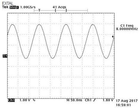
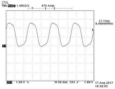
I have 9S12C64CFAE processor (0M66G mask) with Pierce oscillator setup running at 8MHz. For some reason the chip is still running on SCM although the crystal oscillator has nice and full-swing waveforms and starts very fast after the supply voltages are present.
I used BDM to get some information on the register contents and the status register 0x0037 (CRGFLG) shows 0x63 that means that the SCM is active.
I have fundamental 8MHz crystal with 22pF load capacitors (recommended by the crystal manufacturer) and 10M resistor in parallel with the crystal.
As far as I understood, the SCM bit is set purely by hardware and it is not software dependent. Or am I wrong?
So, without any firmware inside the chip should use the external clock (at least when looking at reset values of registers) and not to go into SCM?
Have programmed also the S12SerMon2r1 in using the BDM programmer, but it does not make situation any different...
I have also tried to wire the crystal directly to the chip with associated components to minimize the signal lengths and stray capacitances but the result is still the same.
I really appreciate any help.
Regards, Ville
Solved! Go to Solution.
- Mark as New
- Bookmark
- Subscribe
- Mute
- Subscribe to RSS Feed
- Permalink
- Report Inappropriate Content
- and VDD1 has 5V
And that's perhaps the problem. VDD1 should be similar to VDDPLL. Looks like you shorted it to VDDX/VDDR
Edward
- Mark as New
- Bookmark
- Subscribe
- Mute
- Subscribe to RSS Feed
- Permalink
- Report Inappropriate Content
Hello
Thank you for the answer.
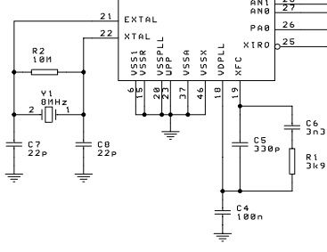
Here is the schematic of the oscillator section.
Test pin (23) is connected to GND as is the \XCLKS (pin 13). C7, C8, C6 and C5 in the schematic are of NP0/C0G type.
I now tried now the same component values as was used on Technologicalarts evaluation board (the schematic is public, on support section: http://support.technologicalarts.ca/docs/Adapt9S12C/AD9S12Csch.pdf )
I have also tried many different crystals and load capacitances, and R2 values between 1 and 10Mohm. All with the same results... Tried also to change the processor. Oscillator should be OK and running because the waveform at XTAL output is OK?
CLKSEL bit 7 is 0 so the PLL is not selected and the bus frequency then should be oscillator / 2. Checked with BDM that 0x0039 (CLKSEL) reads 0x00.
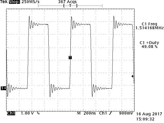
Since it is running at SCM, the pin PE4 shows the self-clock frequency / 2 rather than 4MHz that it should be with the 8MHz crystal.
I will re-calculate the load capacitances with the equations you supplied, but since I have tested so many different component values, I am not expecting much.
Have also tried to feed different frequencies (between 1 and 12MHz) from a function generator to the EXTAL pin as shown by the datasheet (MC9S12C128V1.pdf) picture 11-3, page 345. 2,5V level, of course.
With kind regards,
Ville
- Mark as New
- Bookmark
- Subscribe
- Mute
- Subscribe to RSS Feed
- Permalink
- Report Inappropriate Content
Hi
Did you check voltage at VDDPLL and VDD1? Is regulator working or indeed shorted to VDDX/VDDR?
I would check with probe if /XCLKS is really low.
Edward
- Mark as New
- Bookmark
- Subscribe
- Mute
- Subscribe to RSS Feed
- Permalink
- Report Inappropriate Content
Hello
Done some further measurements.
Voltage on VDDPLL is 2.52V and VDD1 has 5V. Also checked that /XCLKS (pin 13 on this 48LQFP package) is actually tied to ground.
(Actually, tried also /XCLKS signal as 5V but then the crystal oscillator does not start (no waveform on EXTAL and XTAL pins)).
Now it is running but for some reason the Clock Quality Checker does not like it...
With kind regards,
Ville
- Mark as New
- Bookmark
- Subscribe
- Mute
- Subscribe to RSS Feed
- Permalink
- Report Inappropriate Content
- and VDD1 has 5V
And that's perhaps the problem. VDD1 should be similar to VDDPLL. Looks like you shorted it to VDDX/VDDR
Edward
- Mark as New
- Bookmark
- Subscribe
- Mute
- Subscribe to RSS Feed
- Permalink
- Report Inappropriate Content
Hello
Yes, that was the problem! Had a short circuit between those two networks.
Thank you very much for the great advice on troubleshooting, now the bus clock seems to be 4MHz as it should be.
With kind regards,
Ville
- Mark as New
- Bookmark
- Subscribe
- Mute
- Subscribe to RSS Feed
- Permalink
- Report Inappropriate Content
Hi,
is it possible to share schematic design?
Moreover, check (standard mistakes):
- Test pin connected to GND.
- \XCLKS connected to GND for pierce oscillator.
- Load capacitors should be calculated in simplified consideration follows:
The maximal frequency for Pierce oscillator is 40MHz.
The accurate values depend on the features of the crystal presented in the manufacturer's data sheet.
For example - crystal CA-301 has load capacitance = CL >10pF
S12C, S12GC : input pin capacitance for pins XTAL, EXTAL C1i = C2i = 7pF = Ci
Let C3=C4 = Ce
CL = (Ci + Ce)/2 and it has to be >= CL = 10 pF
Then:
(Ci + Ce)/2 >= CL => Ce >= CL*2 - Ci
Ce >= 10pF * 2 - 7pF
Ce >= 13 pF
Rb value is from the interval 100kohm ~ 20Mohm. For low frequency circuits is crystal impedance relatively high and Rb should be high Rb = 10Mohm. For high frequencies (>20Mhz) Rb = 100 kohm.
Rs for high frequencies (>4MHz) can be omitted.
- Test the MCU without setting PLL. Only set PEAR_NECLK=0 and you should se busclk=OSCCLK/2 at the pin PE4.
If it does not help do not hesitate to contact me again.
Best regards,
Ladislav


